Here are the build notes for my PGA2350 Breakout PCB Design.
Warning! I strongly recommend using old or second hand equipment for your experiments. I am not responsible for any damage to expensive instruments!
If you are new to electronics and microcontrollers, see the Getting Started pages.
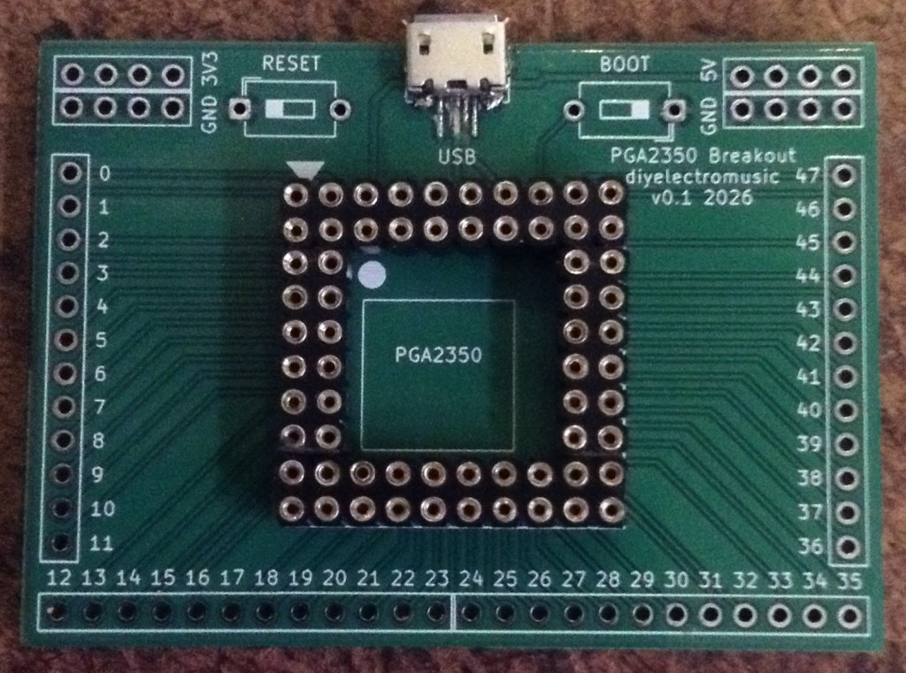
Bill of Materials
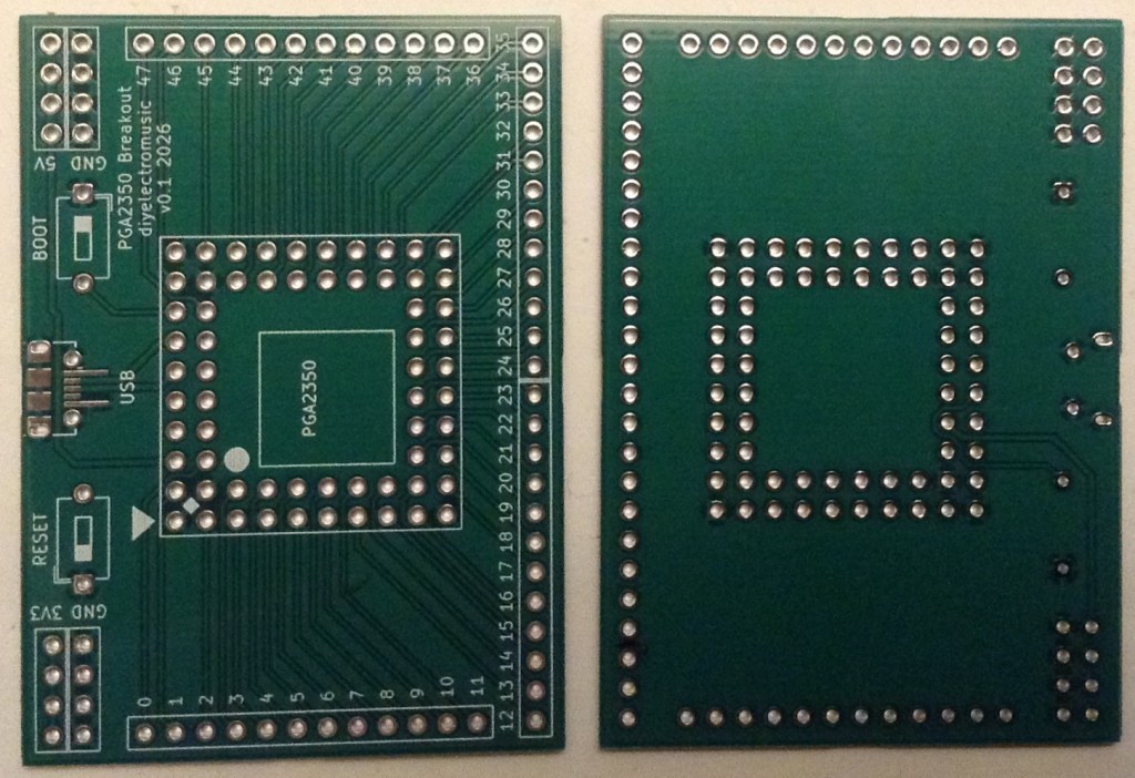
- PGA2350 Breakout PCB (GitHub link below).
- Pimoroni PGA2350.
- SMT micro USB socket (see photos and PCB for footprint).
- 2x 2-pin tactile button switches.
- Double row, round pin header sockets.
- Double row, extended round pin header pins.
- Pin header pins or sockets as required for the breakout.
Reminder: This board is NOT compatible with the similar form-factor Waveshare Core 2350B.
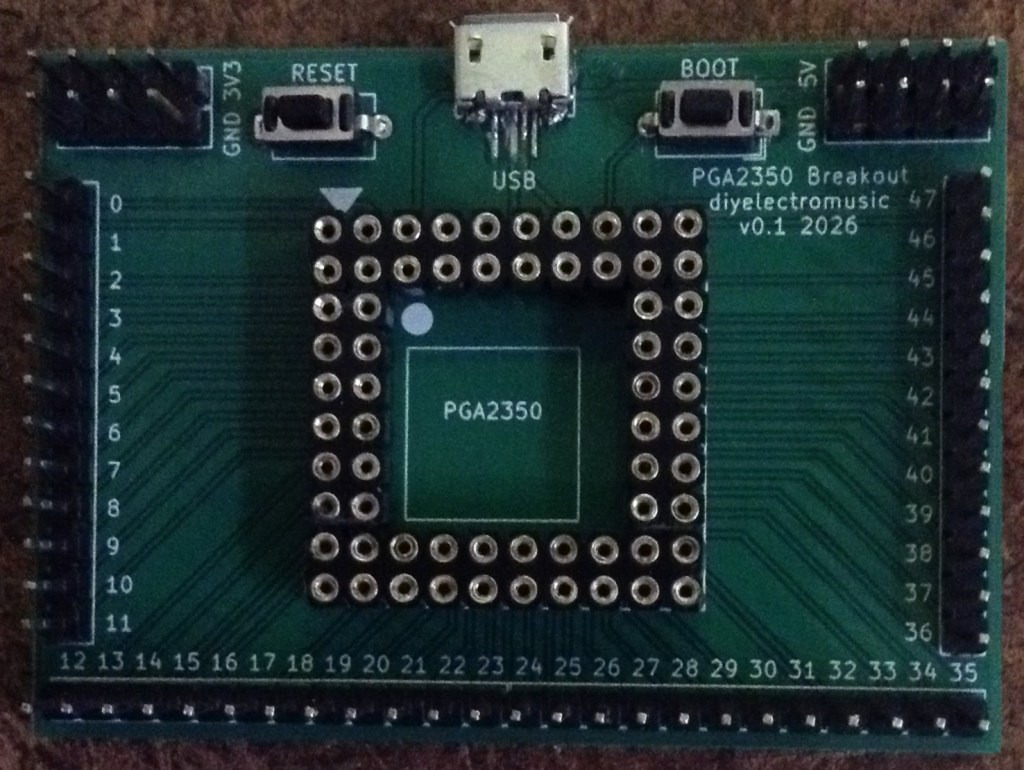
Build Steps
Taking a typical “low to high” soldering approach, this is the suggested order of assembly:
- The micro USB socket.
- The PGA2350 round header pin sockets.
- Switches.
- Pin headers.
I’ve chosen to use pins for the breakout, but pin header sockets would be fine too.
Whilst it makes sense to fit the USB socket first anyway, it is also the most tricky part of the PCB, so if that gets messed up there isn’t much point in carrying on!
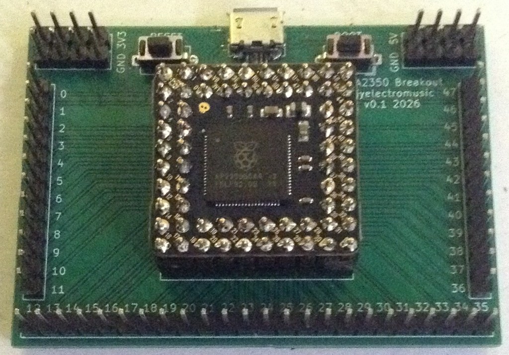
And it was really tricky for me. I’ve soldered them for power before, but this time I needed the data lines connected too. Going slowly, using lots of flux and a magnifying glass seemed to do the trick. I soldered a single case pin connection to hold everything in place whilst attempting the main connections, then tested everything for continuity and lack of shorts before moving on.
When cutting pin header sockets for the PGA2350 socket, they may need filing down on the ends slightly to fit snugly with no bending or forcing when arranged in the square.
Unfortunately the footprint for the buttons didn’t quite match the buttons I had. The holes are slightly too small. I opted to file down the legs of the buttons slightly and then apply a bit more force to get them in place. They went in well enough for me in the end.
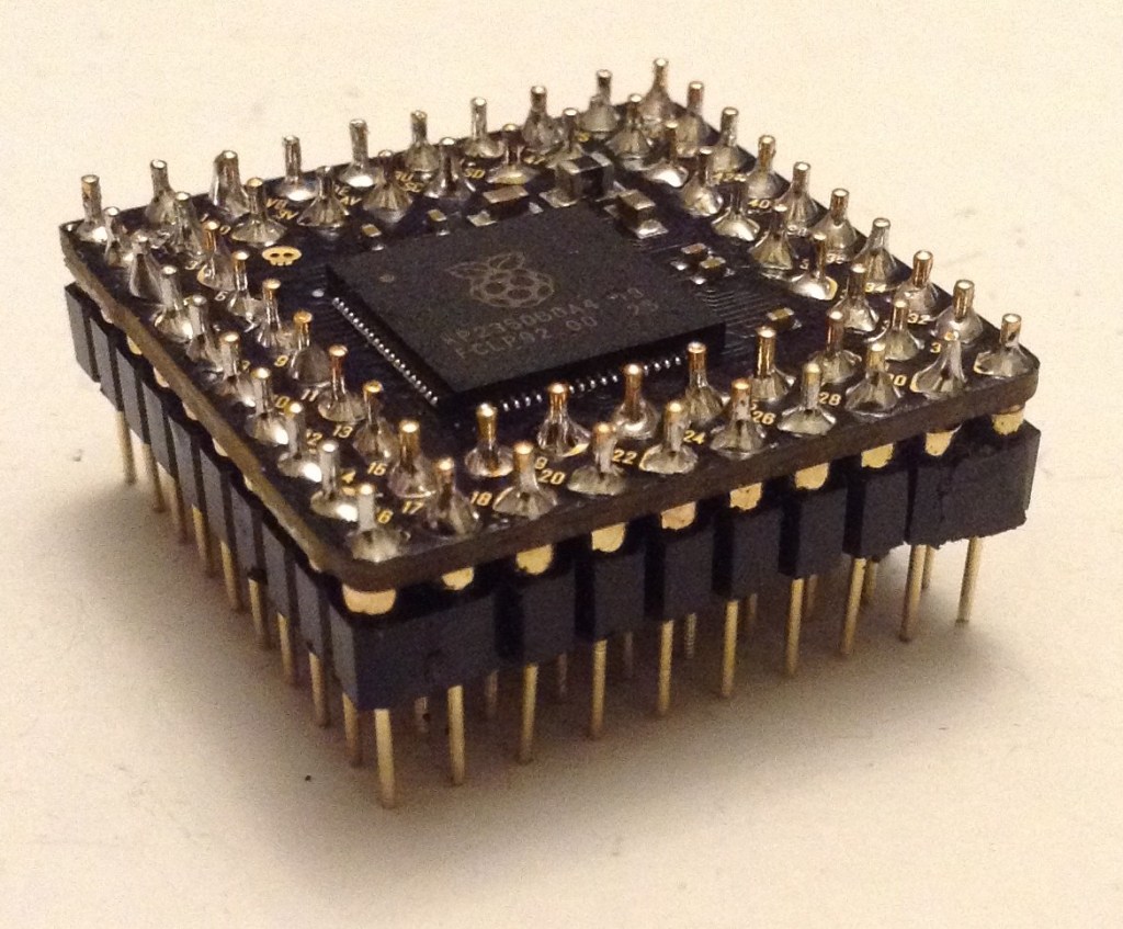
Soldering pins to the PGA2350 itself was quite a hairy moment too. The labels look really cool, but they are not silkscreen, they are gaps in the mask I think. Regardless, solder will stick to them if not careful…
Here are some build photos.
Testing
I recommend performing the general tests described here: PCBs coupled with a thorough visual inspection.
As already mentioned, the USB socket should be checked for continuity and shorts before soldering anything else in place.
When confident everything seems ok, then the board can be connected by USB to a PC and it power up in BOOT mode and the standard RP2350 boot drive should be visible.
PCB Errata
There are the following issues with this PCB:
- As already mentioned the footprints for the buttons have holes that are too small.
Closing Thoughts
The button issue was an annoyance but ok. But I really need to find a better micro USB footprint to use as that was really quite tricky to get right.
The PGA2350, once it has all its pins soldered in place, requires a fair bit of force to fit into the socket, but it isn’t too bad. Getting it back out however isn’t so easy. It can be done with some gentle leverage in the corners, taking care not to bend any pins either on the PGA2350 itself or the breadout board.
But once all assembled and up and running, it seems to work pretty well.
Kevin
