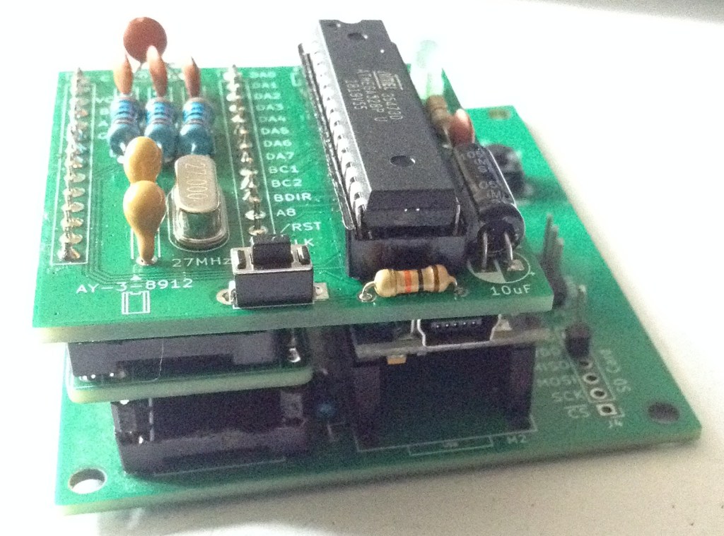
Having explored how an AVR can be used to emulate the AY-3-8912/8910 in AY-3-8912/8910 Hardware Emulation I wanted to have a go at using the very common ATMega328P to do the same. But rather than wire things up on breadboard, I put together a quick PCB to allow me to do some experiments.
Spoilers: This isn’t working yet!! Read on for where I’ve got to, but I’ll need to come back to this at some point.
Warning! I strongly recommend using old or second hand equipment for your experiments. I am not responsible for any damage to expensive instruments!
If you are new to electronics and microcontrollers, see the Getting Started pages.
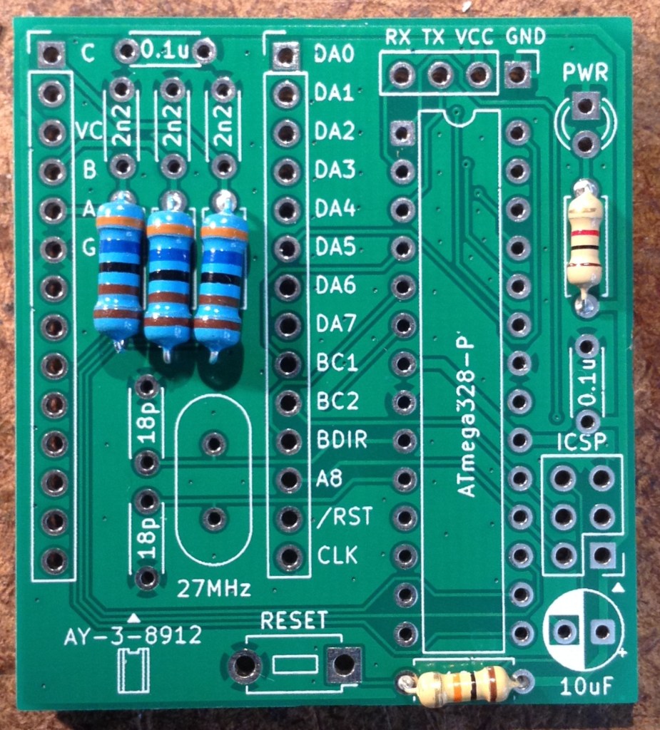
The Circuit
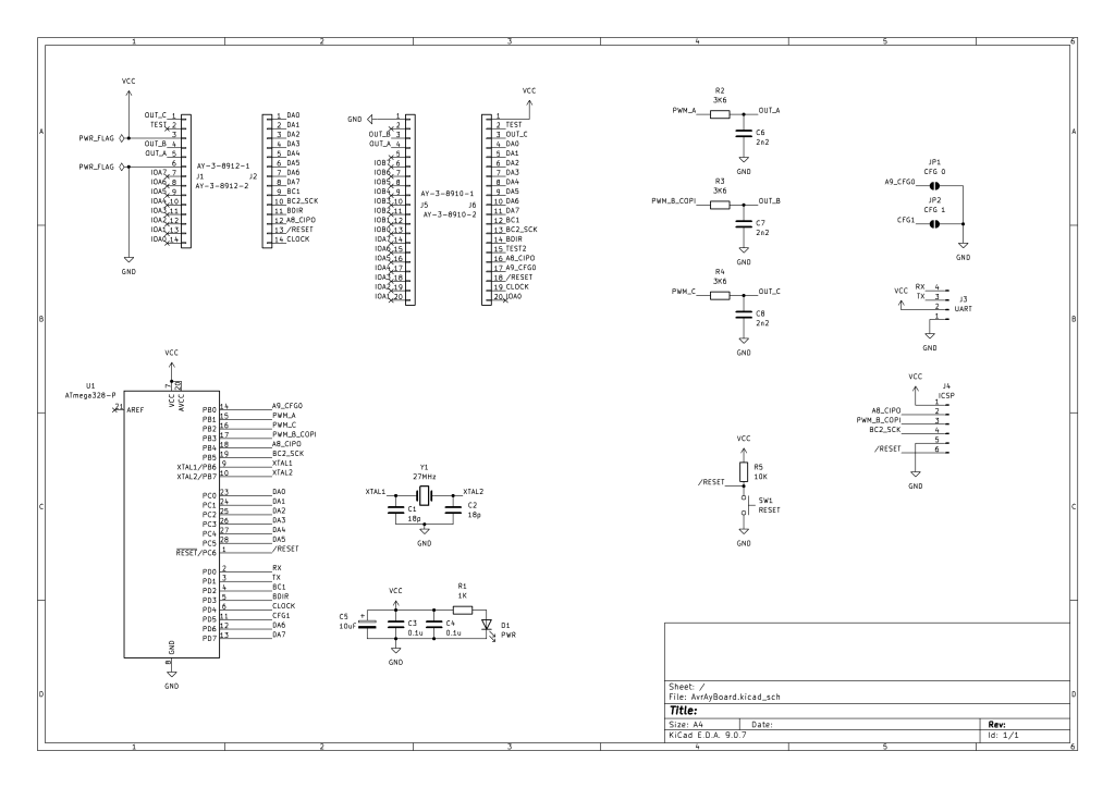
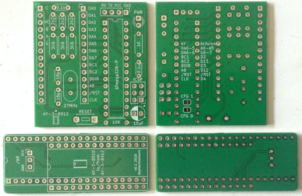
This is essentially the circuit from here: https://github.com/Yevgeniy-Olexandrenko/avr-ay-board
But with an ATMega328P rather than the suggested ATMega48PA (more about that in part one here: AY-3-8912/8910 Hardware Emulation). I’ve included headers for both the AY-3-8910 and AY-3-8912.
I’ve kept the same usage of ATMega ports, which map onto IO for the ATMega328P as follows:
| AY-3-8912 | Schematic | ATMega328P PORT | ATMega328P Pin | Arduino Equivalent |
| D0-D5 | DA0-DA5 | PC0-PC5 | 23-28 | A0-A5 |
| D6-D7 | DA6-DA7 | PD6-PD7 | 12-13 | D6-D7 |
| A8 | A8_CIPO | PB4 | 18 | D12 |
| BC1 | BC1 | PD2 | 4 | D2 |
| BC2 | BC2_SCK | PB5 | 19 | D13 |
| BDIR | BDIR | PD3 | 5 | D3 |
| CLOCK | CLOCK | PD4 | 6 | D4 |
| RESET | RESET | PC6 | 1 | RESET |
| TEST | N/C | |||
| IOA7-IOA0 | N/C | |||
| C | PWM_C | PB2 | 16 | D10 |
| B | PWM_B_COPI | PB3 | 17 | D11 |
| A | PWM_A | PB1 | 15 | D9 |
| A9_CFG0 | PB0 | 14 | D8 | |
| CFG1 | PD5 | 6 | D5 | |
| RX | PD0 | 2 | D0 | |
| TX | PD1 | 3 | D1 | |
| VCC | VCC | VCC | 7, 20 | VCC |
| GND | GND | GND | 8 | GND |
The only change is I’m not connecting TEST to anything. I’ll have to see if this becomes an issue later…
The circuit calls for overclocking the ATMega328P to 27MHz (again more discussion on this in the first part).
I’ve included breakout headers for ICSP and a serial header and have swapped the oscillator to a crystal using a common configuration I’ve seen on many DIY Arduino-style boards using an ATMega328P.
Rather than put together two boards, one for the 8912 and one for the 8910, I’ve also put together a simple adaptor circuit to allow one to plug into the socket for the other.
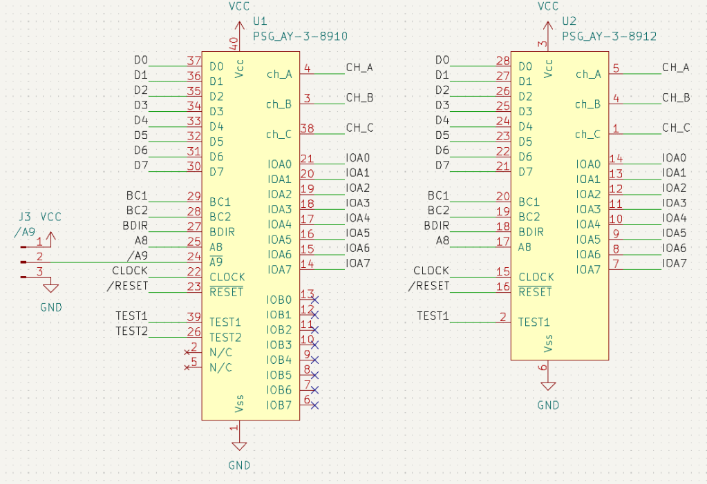
The schematic essentially just maps the signals from one footprint onto the other.
The only slight complication is that /A9 for the 8910 doesn’t exist on the 8912, so I’ve left in a jumper to provide the option of tying this to GND or VCC should the need arise. This should allow the larger 8910 to be used in the place where a 8912 is required whilst still enabling the 8910.
PCB Design
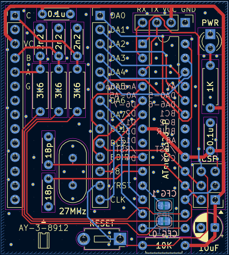
I did wonder quite how much of a 28 pin DIP could fit inside the footprint of a 28 pin WDIP and still keep through hole components, but I didn’t have to wonder for long to see it wasn’t really going to work.
So as this is basically just for messing around I went with the format as shown. This way, round-profile pin headers can be used on the underside for the AY footprint if the board is to replace a genuine device. Alternatively normal pin headers or sockets can be used on the topside if jumper wires are going to be used to hook this board into another PCB.
The two CFG jumpers are solder bridges (default not connected) on the underside of the board. I’ve also listed the Arduino versions of the AVR pins used on the underside too.
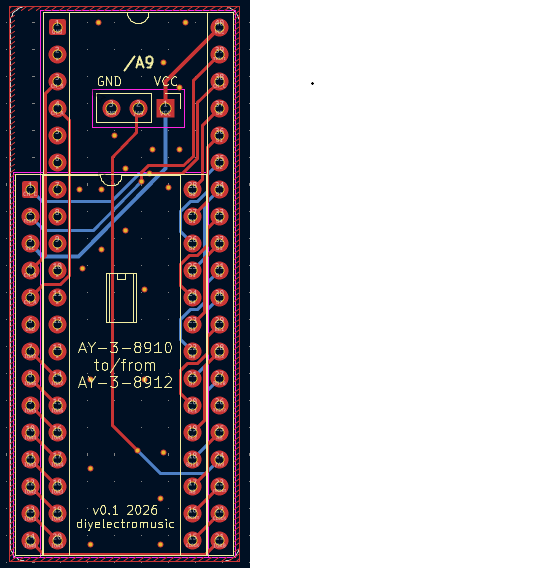
For the converter board, I’ve left the /A9 jumper as standard pin headers. With hindsight I’m not sure when this would be wanted to be tied high, as presumably that would disable the chip. When plugging a 8912 into a 8910 socket, anything expecting an 8910 and using /A9 as part of the addressing scheme would require some additional logic before mapping it onto the smaller 8912.
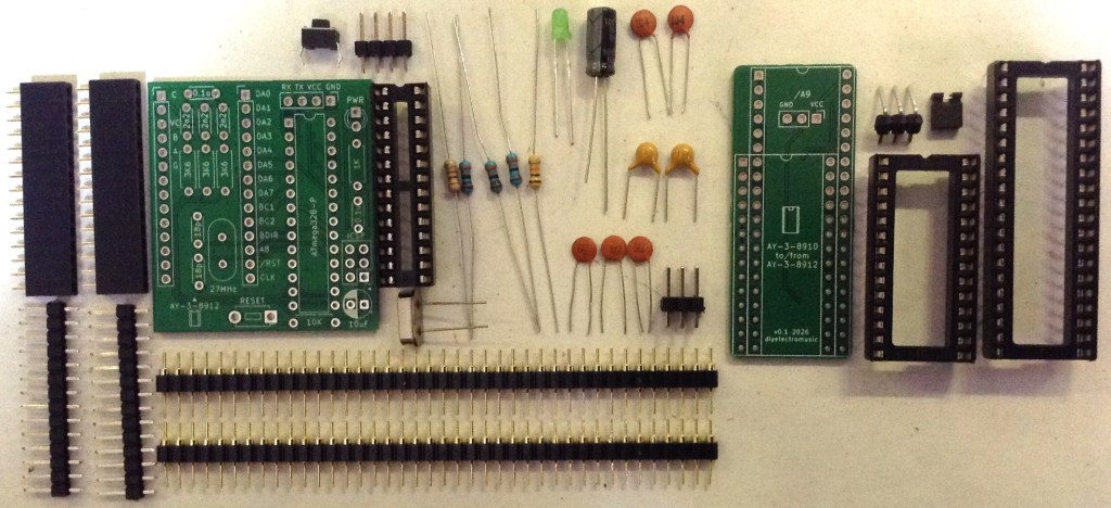
Bill of Materials
AVR-AY Emulator Board:
- AVR-AY-Board PCB (GitHub link below).
- ATMega329P (28 pin DIP version).
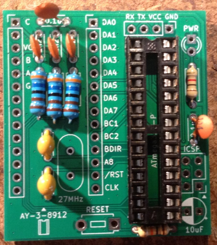
- 1x 1K resistor
- 3x 3K6 resistors
- 1x 10K resistor
- 1x 10uF electrolytic capacitor
- 2x 100nF ceramic capacitors
- 3x 2.2nF ceramic capacitors
- 2x 18pF ceramic capacitors
- 1x 3mm LED (colour to taste)
- 1x 27 MHz crystal (2 pin, low-profile, HC-49 package – see footprints)
- 1x 2-pin momentary push switch (see footprints)
- Optional: 28-way narrow DIP socket
- Optional: round-pin header pins (see photos and discussion)
- Range of pin headers or sockets as required
AY-3-8910 to 12 Converter:
- AY-3-8910-12 Converter PCB (GitHub link below).
- Either 40-pin WDIP socket or 28-pin WDIP socket.
- Round-pin header pins.
AY-3-8910 to 12 Converter Build
This is a relatively straight forward build, but depending on the DIP sockets used it might be necessary to doctor the socket slightly to sit neatly over the soldered pins.
Order of build:
- Round pins for either the 28 pin or 40 pin part of the PCB.
- The 40 pin or 28 pin DIP socket.
If the converter is from a 8912 socket to a 8910 device, then the /A9 jumper or a solder link will have to be configured, presumably connecting it to GND to make it permanently active.
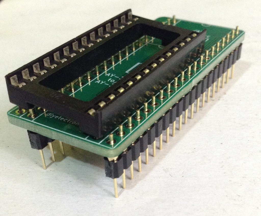
One note of caution – the pins I was using are not particularly robust, so when removing the adaptor from its socket, I managed to break one and had to replace it, which wasn’t easy.
But apart from that, it works!
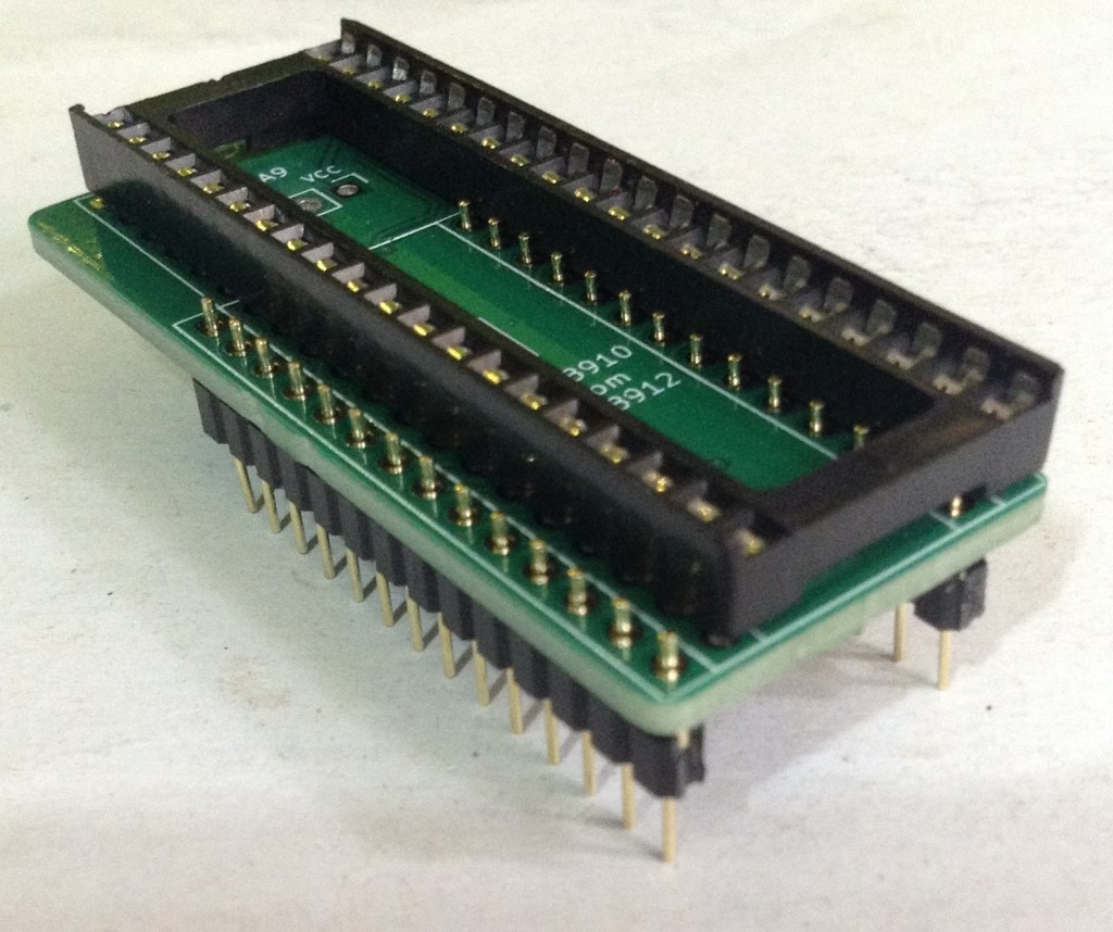
AVR AY Board
As already mentioned there are a number of configuration options for the 28-pin AY-3-8910 emulation as illustrated below.
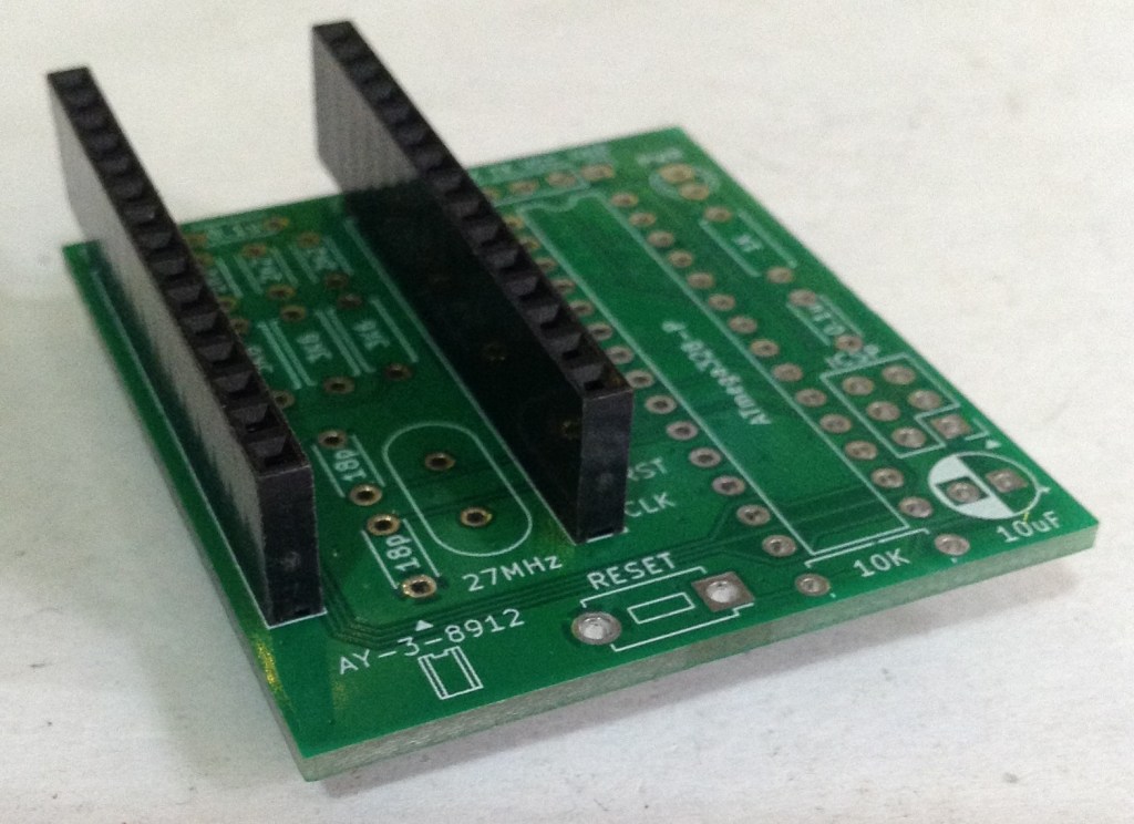
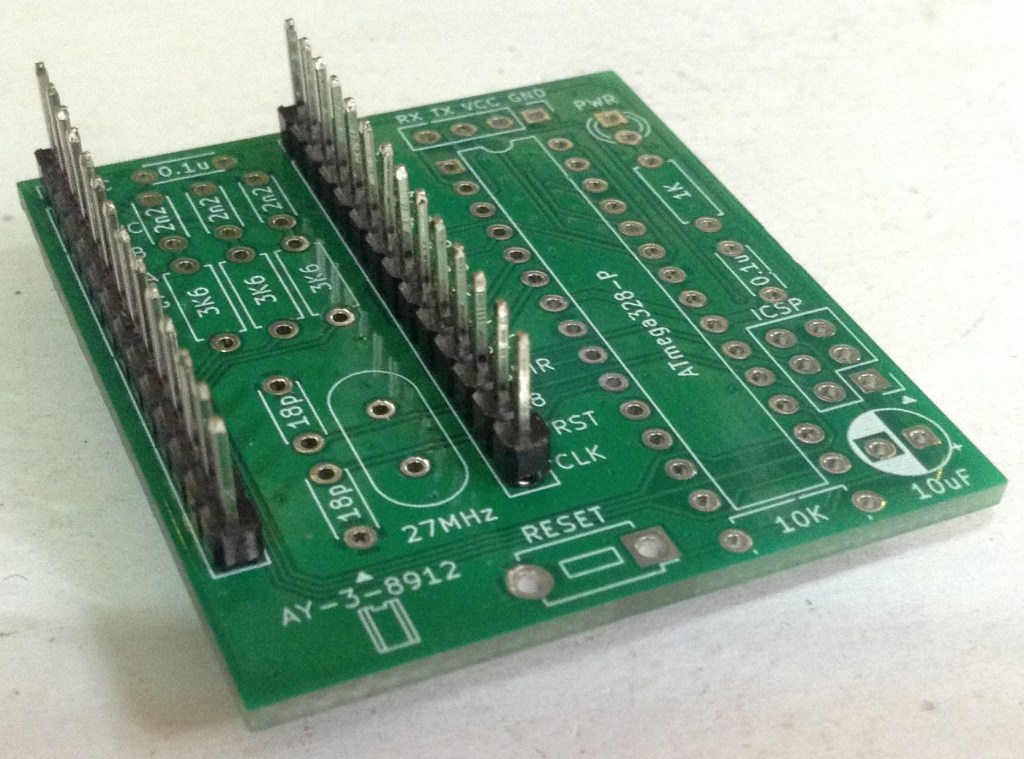
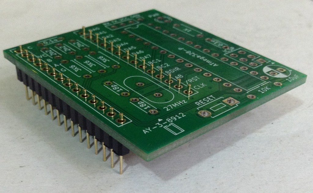
The first two are designed for jumper wire connections. The third shows the use of pins which would allow the board, space permitting, to be inserted into a AY-3-8910 socket on an existing board.
These headers will be soldered on last, but it is worth deciding in advance what configuration will be required.
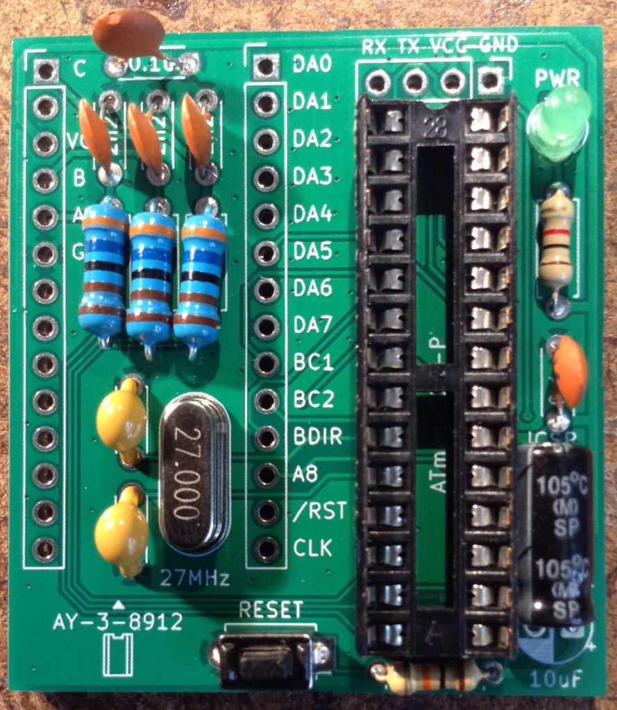
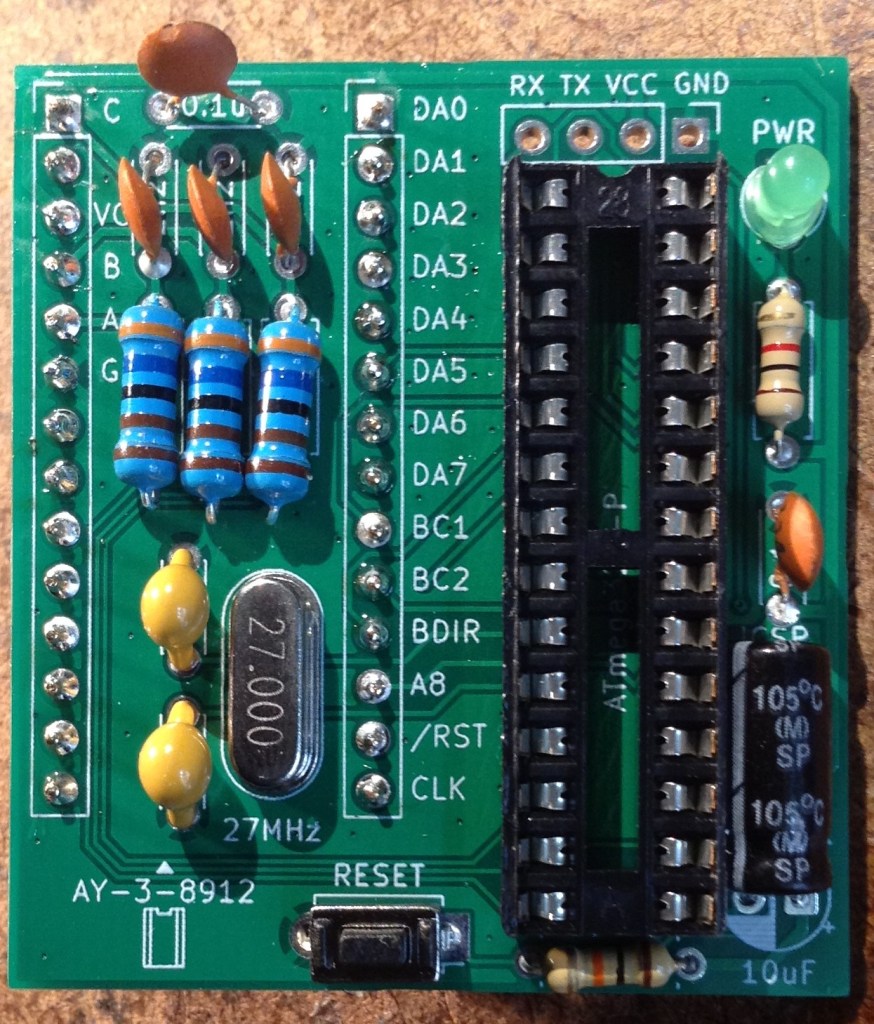
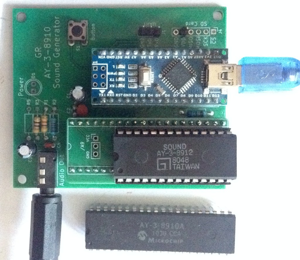
I’ve chosen not to populate the UART and ICSP headers, and am using round pins so that this can hopefully replace an AY-3-8912. But at the moment all my test boards are built for the AY-3-8910, so I’m also having to use the converter, which has led to the following stack of boards!
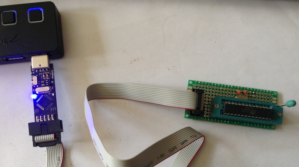
ATMega328P Programming
The stand-alone ATMega328P chip cannot be programmed directly from the Arduino IDE with this code as it stands. Instead the following are required:
- AVRDude: https://github.com/avrdudes/avrdude
- An AVR Programmer: I’m using a cheap USBasp clone, so one based on this: https://github.com/piit79/USBasp
- Connection to the device via ICSP: I’m using a homemade link, but it should be possible to use the ICSP header on the PCB; plug it into a DIP-version of another Arduino Uno board; or possibly even a second Arduino Uno board in “Arduino as ISP” mode.
The firmware should be downloaded from https://github.com/Yevgeniy-Olexandrenko/avr-ay-board.
Update: I ended up using a slightly different firmware and configuration – see later…
I’m using v1.0 of the firmware and have downloaded the binary firmware and the 1.75MHz configuration. I now have the following files:
C:\Kevin\Temp> dir
09/05/2026  15:49    <DIR>          .
09/05/2026  15:49    <DIR>          ..
09/05/2026  15:49             1,920 avr-psg.hex
09/05/2026  15:40           909,660 avrdude.conf
09/05/2026  15:40         9,604,608 avrdude.exe
09/05/2026  15:40        13,316,096 avrdude.pdb
09/05/2026  15:49                34 config-1.75mhz.hex
C:\Kevin\Temp>
To program the ATMega328P requires the following instructions to get the code into flash, the configuration into EEPROM and to set the fuses for the MCU:
C:\Kevin\Temp>avrdude -c USBasp -p ATMega328P -U flash:w:avr-psg.hex:i
Error: cannot set sck period; please check for usbasp firmware update
Error: cannot set sck period; please check for usbasp firmware update
Reading 682 bytes for flash from input file avr-psg.hex
Writing 682 bytes to flash
Writing | ################################################## | 100% 0.43 s
Reading | ################################################## | 100% 0.23 s
682 bytes of flash verified

Avrdude done.  Thank you.


C:\Kevin\Temp>avrdude -c USBasp -p ATMega328P -U eeprom:w:config-1.75mhz.hex:i
Error: cannot set sck period; please check for usbasp firmware update
Reading 5 bytes for eeprom from input file config-1.75mhz.hex
Writing 5 bytes to eeprom
Writing | ################################################## | 100% 0.09 s
Reading | ################################################## | 100% 0.01 s
5 bytes of eeprom verified

Avrdude done.  Thank you.

C:\Kevin\Test>avrdude -c USBasp -p ATMega328P -U lfuse:w:0xdf:m -U hfuse:w:0xdf:m -U efuse:w:0xfd:m
Error: cannot set sck period; please check for usbasp firmware update

Processing -U lfuse:w:0xdf:m
Reading 1 byte for lfuse from input file 0xdf
Writing 1 byte (0xDF) to lfuse, 1 byte written, 1 verified

Processing -U hfuse:w:0xdf:m
Reading 1 byte for hfuse from input file 0xdf
Writing 1 byte (0xDF) to hfuse, 1 byte written, 1 verified

Processing -U efuse:w:0xfd:m
Reading 1 byte for efuse from input file 0xfd
Writing 1 byte (0xFD) to efuse, 1 byte written, 1 verified

Avrdude done.  Thank you.
The error “cannot set sck period” is apparently pretty common especially with USBasp clones, and can be ignored.
The three fuse settings come from the original AVR-AY firmware (here) in the readme as follows:
ATMEGA328 ===================================================
	avrdude -p m328p -c USBasp -U flash:w:AY_Emul_XXX_Nch_KK_MM.hex -U eeprom:w:Conf_XXX_YYMHz_ZZMhz.hex -U lfuse:w:0xee:m -U hfuse:w:0xdf:m -U efuse:w:0xfd:m
Example:
	avrdude -p m328p -c USBasp -U flash:w:AY_Emul_250_2ch_m328_ay.hex -U eeprom:w:Conf_standard_27MHz_1_75Mhz.hex -U lfuse:w:0xee:m -U hfuse:w:0xdf:m -U efuse:w:0xfd:m
=============================================================
But where the fuse settings for lfuse = 0xEE, when decoded from the ATMega328P datasheet and an online AVR fuse calculator here: https://eleccelerator.com/fusecalc/fusecalc.php?chip=atmega328p means the following:
0xEE = b1110 1110
CKDIV8 = 1 (unprogrammed)
CLKOUT = 1 (unprogrammed)
SUT    = 10
CLKSEL = 1110
Which from the AVR fusecalc site maps onto:
- External crystal oscillator
- Frequency 8MHz +
- Start up time 1K
- Powerdown/reset 16
However, following through the settings in the datasheet, it is similar but slightly different, giving:
- Low power crystal oscillator (CLKSEL3:0 = 1111 – 1000)
- Low power operating mode 111 = 8.0-16.0 MHz (with recommended caps 12-22pF)
- CLKSEL0+SUT = 0+10 = Ceramic Resonator BOD enabled, Start up time 1KCK, additional delay 14CK
But I’m not using a ceramic resonator, I’m using a crystal oscillator, so I think I need the mode:
- Crystal oscillator BOD enabled, startup time 16KCK, additional delay 14CK = CLKSEL0+SUT = 1+01
There is no “1KCK” for the crystal oscillator settings, so I’ll have to use 16KCK I guess?
This is what gives me the 0xDF value I’ve used:
0xDF = b1101 1111
CKDIV8 = 1 (unprogrammed)
CLKOUT = 1 (unprogrammed)
SUT    = 01
CLKSEL = 1111
Actually, this wasn’t working with either 0xEE or 0xDF, so I decide to try to turn off BOD and went with “slow rising power” (CLKSEL0+SUT = 1+11) which gave me the fuses:
lfuse = b1111 1111 = 0xFF
hfuse = 0xDF (as before)
efuse = 0xFF (no brown-out detection)
But that isn’t working either…
The AY891x Library and BCn/BCDIR control
Eventually, I remembered reading about the control signals with the library that was designed for use with that test board. It states the following (here):
“While the PSG has tight timing requirements, it is possible to use digitalWrite() by using all three bus control signals (BDIR, BC1, BC2) and cycling through an extra state when reading and writing the chip registers.”
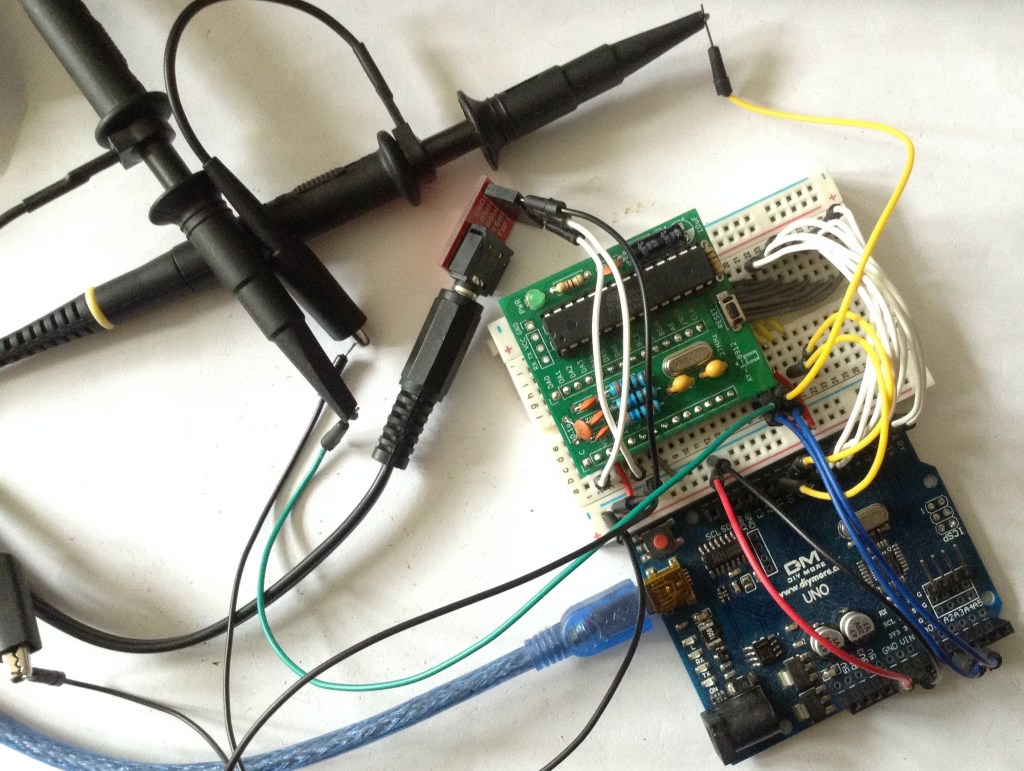
But the emulation is ignoring BC2 (more here), relying instead on the ATMega’s two IO interrupt pins INT0 and INT1 on D2 and D3, to trigger on BDIR and BC1. This means I had to ditch the library and instead switched over to my own PORT IO driver as described here: Arduino and AY-3-8910 – Part 3.
Resetting the fuses as before, unfortunately it still isn’t working.
At this point I loaded on a simple tone() function on one of the IO pins using the Arduino IDE then set the fuses again as above. I can definitely see that the frequency for the tone() output is almost twice as high as when the ATMega328P is plugged into the Arduino, so the 27MHz crystal is certainly having an effect compared to the Uno’s original 16MHz.
I can also see the 105kHz PWM carrier frequency on all three PWM output pins, but the peaks are so narrow, these must be responding to a level 0 output which implies all code is working, but there are simply no register writes getting through.
So, in summary, I think the code on the emulator is running fine – so why isn’t it responding to register writes?
An Epiphany?
At this point I left things for a bit and came back to it all a few days later.
I was chewing over why the register writes didn’t seem to be getting through, so at this point I think the handling of BC1 and BDIR are key. The next things that I tried:
- Getting it all on a breadboard and showing it working with a real AY-3-8910.
- Check I can see BC1 and BDIR and the data lines doing something.
- Replace the real chip with the emulator.
- Repeat the tests for BC1, BDIR and data – all appear ok.
At this point I’m suspecting the interrupts aren’t getting through (remember BC1 and BDIR are triggered off the external interrupts), so I’m contemplating two things:
- Some test code that lights an LED on an external interrupt.
- Porting the whole code across to the Arduino environment to let me build and run it all from there.
But this has got me wondering about build differences for the two devices – what might be different between the ATMega48 and ATMega328P. Would rebuilding from source for the ATMega328P sort it out?
Looking at the original code, I can see there are many different binaries for the different chips. For the repository I’m using there is just one.
Looking in the two chip datasheets, I can see that the INT0 interrupt vector is different – it is 2 (address 0x001) for the 48 and whist it is still 2 for the 328P, the address is 0x0002. From the 48 datasheet:
“Each interrupt vector occupies two instruction words in ATmega168, and one instruction word in ATmega48 and
ATmega88.”
From the 328P datasheet:
“Each interrupt vector occupies two instruction words in Atmel ATmega328P.”
Looking at the suggested implementations of the vector tables, they are shown as follows:
// ATMega48 vector table
0x000 rjmp RESET      ; Reset Handler
0x001 rjmp EXT_INT0   ; IRQ0 Handler
0x002 rjmp EXT_INT1   ; IRQ1 Handler

// ATMega328P vector table
0x0000 jmp RESET      ; Reset Handler
0x0002 jmp EXT_INT0   ; IRQ0 Handler
0x0004 jmp EXT_INT1   ; IRQ1 Handler
So presumably one is a relative jump (rjmp) which is a single word (16-bit) instruction, vs an absolute jump which is a two-word (32-bit) instruction.
With hindsight is seems obvious I’d need to rebuild for the ATMega328P, but the initial talk of compatibility lulled me into a false sense of security!
There is no build for the 328P in the listed repository, but going back to the original avr-ay source, there are builds for all supported MCUs, each with variants covering:
- 2 or 3 channel sound.
- AY or YM volume tables.
- Additional speaker output on PD1.
There are configuration options for:
- Serial, parallel, or both (“standard”).
- 1.75MHz, 1.78MHz, or 2.0MHz operation.
- 20MHz to 40MHz (including my required 27MHz).
I’ve now downloaded:
avrdude -c USBasp -p ATMega328P -U flash:w:AY_Emul_260_3ch_m328_ay.hex:i
avrdude -c USBasp -p ATMega328P -U eeprom:w:Conf_parallel_27MHz_1_78Mhz.hex:i
avrdude -c USBasp -p ATMega328P -U lfuse:w:0xee:m -Uhfuse:w:0xdf:m -U efuse:w:0xfd:m
But unfortunately it still isn’t working…
I did notice in the original source, a number of conditional assembler code, based on the initial configuration of MCU_TYPE. But most of it is of the form “if MCU_TYPE==0” which is giving alternative code for the ATMega8. There is one piece of code that implies something different for the ATMega48:
	; get byte 0 from EEPROM, check value > 0 or skip USART initialization if value = 0
#if MCU_TYPE == 0 ||  MCU_TYPE > 1
	out		EEARH,C00		; is absent in Atmega48
#endif
	out		EEARL,C00
I also note that the vector table is all relative jumps:
	.cseg
;------------------------------------------------------
; INTERRUPT VECTORS TABLE
;------------------------------------------------------
	.org	0x0000
	rjmp	_RESET

	.org	INT0addr
	rjmp	_INT0_Handler

	.org	INT1addr
 	rjmp	_INT1_Handler

	.org	URXCaddr
	rjmp	_USART_RX_COMPLETE
But as each entry has its own origin statement, one presumes that these are correct for the MCU type.
Double checking the hex records for my chosen firmware, and adding some expansions and annotations, I can see:
// Format:
// :ll aaaa tt dd..dd cc
//                    ++-- CRC
//             +----+----- Data
//          ++------------ Record type
//     +--+--------------- Address
//  ++-------------------- Data length

:02 0000 02 0000 FC  // tt=02: Extended (Upper) Segment Base Address

// Vector Table tt=00: Data
:02 0000 00 88C0 B6
:02 0004 00 4AC0 F0
:02 0008 00 56C0 E0

// Start of code/data tt=00; Data
:10 0048 00 50C0000101010202030506090D11161D 29
:10 0058 00 242D0000010101010101020202020303 33
:10 0068 00 0505060607090B0D0F111316191D2024 87
...
:10 02F8 00 0092880010928A0092CF05910D932A95 5A
:04 0308 00 E1F70895 7C
:00 0000 01 FF       // tt=01: End of File
So yes, it would appear that the vectors in the vector table are indeed on the expected 32-bit boundaries which matches and it has values for vectors 2 and 3, so INT0 and INT1. Vector 1 is RESET.
One oddity, each record is only 2 bytes long, so I guess it is assuming that the missing bytes will be zero? Really, the full records should perhaps be:
:04 0000 00 88C00000 B4 // Needed to recalc CRC
:04 0004 00 4AC00000 EE
:04 0008 00 56C00000 DE
I don’t know the algorithm for calculating the CRC, but I don’t need to. When attempting to download via avrdude any CRC mismatch is reported, detailing what value was expected which allows me to set the correct value for each line at a time!
But as these are instructions rather than addresses themselves, maybe it would be fine. If the PC hits this address, then the instruction will be (presumably) a rjmp which is only two bytes and all would be fine.
But regardless, unfortunately this still isn’t working. I’m now at quite a loss as to what to try next.
I did go back and look at the original firmware I was using and it has the following:
:06 0000 00 70C039C045C0 CC
So I don’t see how this would work on an ATMega328P at all as each vector is only half the expected size.
The reset vector is probably ok, as the first two bytes will be read as a “rjmp” instruction and presumably the next two bytes ignored. But INT0 and INT1 will be jumping off into who-knows-where.
This would match the evidence that the board seems to get initialised but no register writes are processed.
So this at least does confirm that the original firmware was no good for me.
Conclusion
I’ve got to draw a line under this for now. I’m going to hit publish on this post as is, and put this aside for a bit.
Some possible future directions:
- Solder on the ICSP header to make uploading code a bit easier.
- Load up some simple Arduino firmware that will indicate if INT0/INT1 are actually getting through.
- Create a ATMega48 breakout to see if the board would work with the original MCU ok.
- I’m still not convinced with that clock – it seems a very low amplitude – I wonder if those capacitors are the right values.
- Port the whole lot to the Arduino environment. This is going to be a fair bit of work as you can’t use assembler directly, but only via asm(“nop”) style directives…
But for now, this one is on pause.
Kevin
