This project uses my EuroRack 6HP MCU Experimenter Module to implement HAGIWO’s Arduino Nano based VCO.
This post describes how to put it together and test the basic functionality. Future posts will look at some code that can run on the module (see the “Sample Applications” section).
Warning! I strongly recommend using old or second hand equipment for your experiments. I am not responsible for any damage to expensive instruments!
These are the key tutorials for the main concepts used in this project:
- HAGIWO’s Arduino Mozzi VCO Module
- HAGIWO’s Arduino Mozzi FM VCO
- My EuroRack 6HP MCU Experimenter Module Usage Notes
If you are new to Arduino, see the Getting Started pages.
Parts list
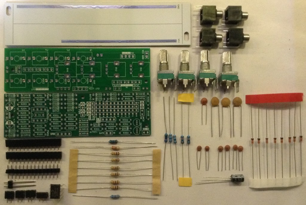
- Arduino Nano
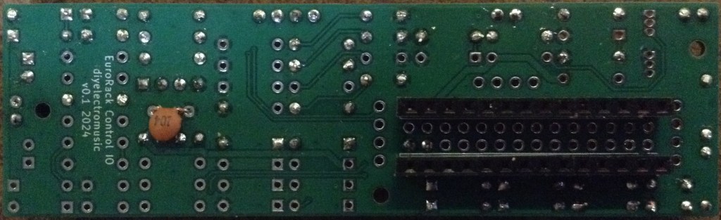
- EuroRack 6HP MCU Experimenter Module Arduino MCU board.
- EuroRack 6HP MCU Experimenter Module IO board built as described below.
- EuroRack 6HP MCU Pots and Jacks PCB built as described below.
- Blank 6HP front panel.
- M2 mounting screws, fixings, nuts.
For the IO board:
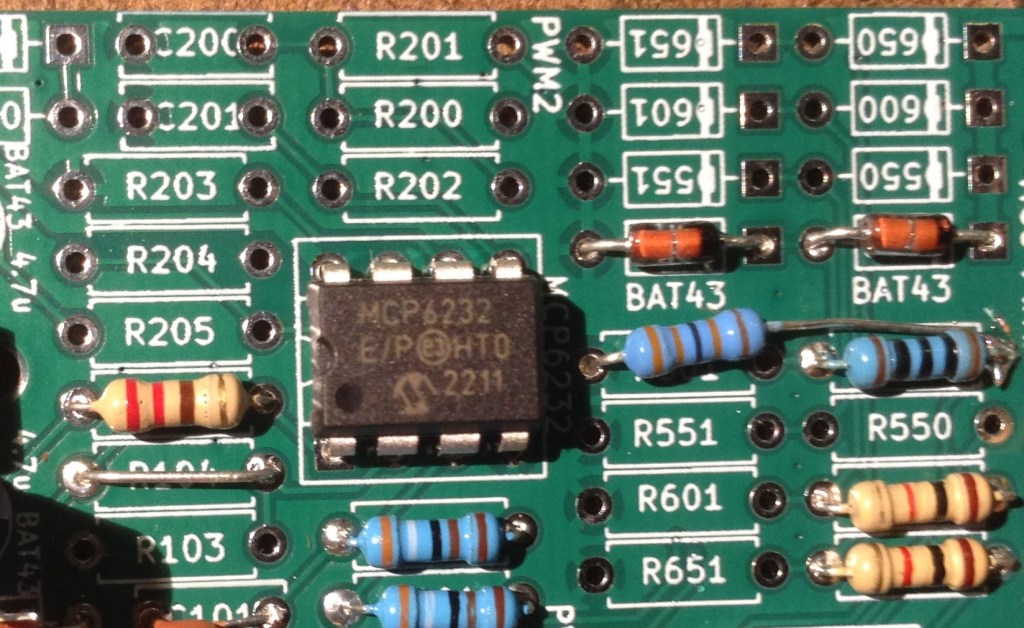
- 1x MCP6232 or equivalent OpAmp.
- 8x BAT43 Schottky diodes.
- Normal resistors: 1x 100Ω, 1x 200Ω, 4x 1kΩ, 1x 330kΩ, 2x 100kΩ.
- Higher accuracy resistors (1% or better): 2x 3.9kΩ, 1x499kΩ.
- Ceramic Capacitors: 4x 100pF, 1x 4.7nF, 1x 10nF, 3x 68nF, 1x 100nF.
- Electrolytic Capacitors: 1x 4.7uF.
Note: it is worth measuring a range of 499K and 3.9K resistors and finding the best ones. In my case I only had 500K resistors, so found the closest to 499K I had. I ended up with two 3.88K and one 498K.
For the Pots and Jacks board:
- 4x 10kΩ or 100kΩ PCB mount potentiometers.
- 4x “Thonkiconn” jack sockets.
- Header pins.
- Jumper wires
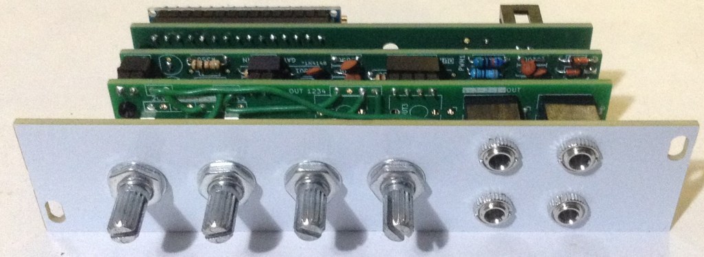
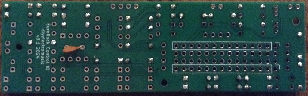
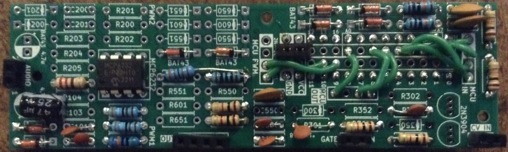
The IO Board
Here is how the various sub-circuits of the IO board will be used:
| Circuit Element | IO Board Connection | Function |
| R/C 40x | CV_IN 1 | Control Voltage 1 |
| R/C 45x | CV_IN 2 | Control Voltage 2 |
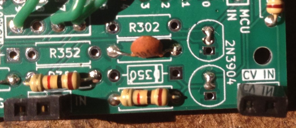
| R/C 30x | GATE_IN 1 | Potentiometer Input 1 |
| R/C 35x | GATE_IN 2 | Potentiometer Input 2 |
| R/C 65x | OUT 4 | Potentiometer Input 4 |
| R/C 60x | OUT 3 | Potentiometer Input 3 |
| R/C 55x | OUT 2 | Not used |
| R/C 50x | OUT 1 | 1V/Oct Control Voltage |
| R/C 10x | PWM 1 | Audio output |
| R/C 20x | PWM 2 | Not used |
Notice that the GATE and OUT circuits are being used in “alternative” modes as additional inputs (see the Usage Notes for more details). In particular the transistors on the GATE circuits are not used.
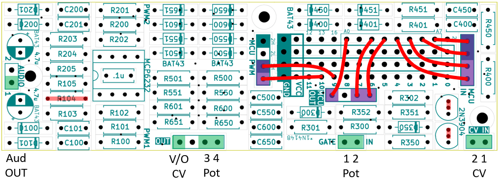
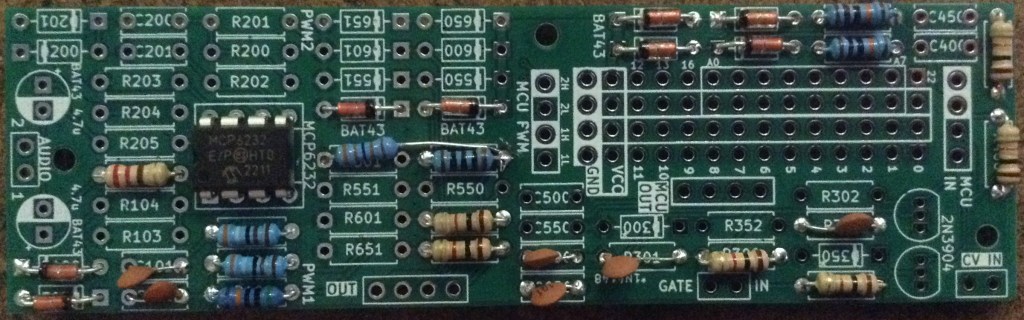
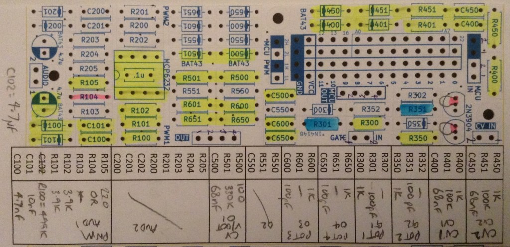
The following shows which components of the PCB will be populated (yellow), which will be changed for other components (blue), which wire links are required (red) and which connectors will be used for linking to the Pots and Jacks board (green) and MCU (purple).
Here is the list of components required for the above:
Resistors:
- R100: 499K
- R101, R102: 3.9K
- R105: 200Ω
- R300, R350, R400, R450, R600, R650: 1K
- R401, R451: 100K
- R500: 100Ω
- R501: 330K
Capacitors
- C100: 4.7nF
- C101: 10nF
- C102: 4.7uF electrolytic
- R301, R351, C400, C450, C600, C650: 100pF (yes, two resistor slots are capacitors).
- C400, C450, C500: 68nF
Other:
- D100, D101, D400, D401, D450, D451, D500, D501: BAT43 Schottky Diodes
- MCP6243
The mapping between IO connections and MCU IO pins is as follows (all other IO pins are not used):
| MCU Connection Point | MCU IO Link | Function |
| MCU PWM 1H | 9 | Audio OUT |
| MCU PWM 1L | 10 | Audio OUT |
| MCU IN CV 2 | A7 | CV2 |
| MCU IN CV 1 | A6 | CV1 |
| MCU IN GATE 2 | A5 | Pot 2 |
| MCU IN GATE 1 | A4 | Pot 1 |
| MCU OUT 4 | A3 | Pot 4 |
| MCU OUT 3 | A2 | Pot 3 |
| MCU OUT 1 | A0 | 1V/Oct CV |
Note: the order of the Gate/CV is (from top to bottom): CV 2, CV 1, G2, G1. The ordering of the OUT connections is the same for both sets of pin headers: 1 on the left, through to 4 on the right.
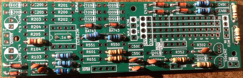
Build Order and Photos
This is the suggested build order:
- Diodes.
- Resistors.
- Small capacitors.
- Header sockets (assuming PH5 and PH3.5 sockets).
- Capacitor on the rear of the board.
- OpAmp.
- Larger capacitors.
- MCU board header sockets on rear of the board.
- Jumper wires.
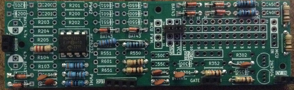
When installing R501, I’ve opted to make the fix described in the EuroRack 6HP MCU Experimenter Module Usage Notes and swap its position to the other side of R500 as shown below.
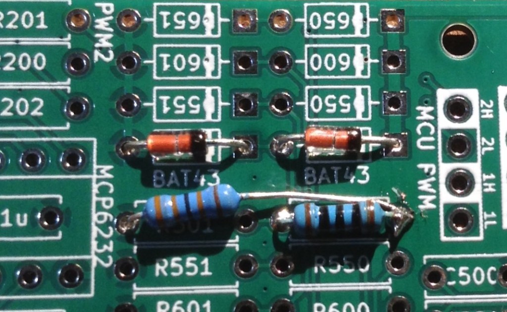
Otherwise the build proceeding pretty much as suggested.
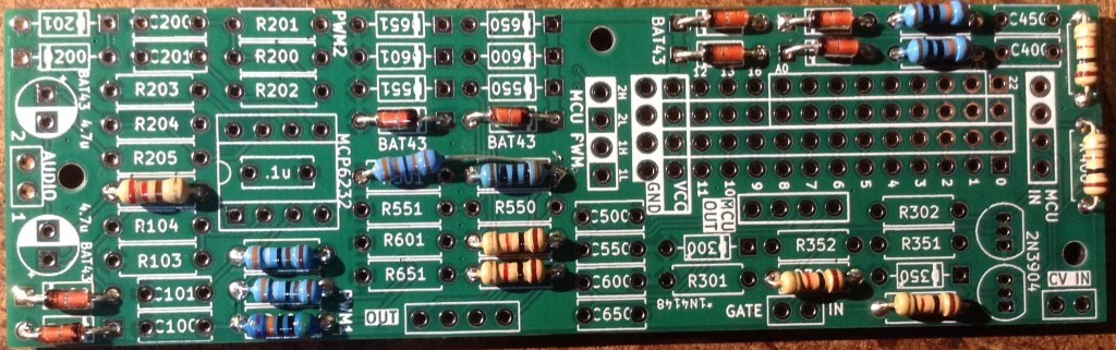
Note that the OpAmp’s capacitor must be soldered to the rear of the board prior to fixing the OpAmp.
The install the OpAmp, smaller headers and larger capacitors.
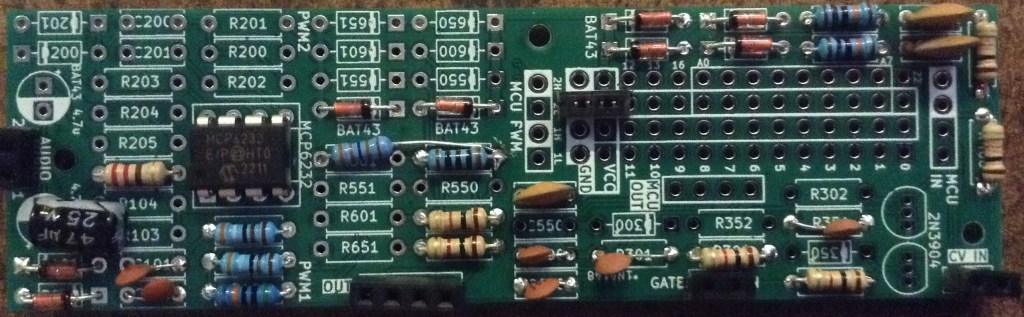
Finally the longer headers for the MCU board can be installed on the rear of the board.
Finally the patch links can be installed as described previously (including the links instead of R104 and the transistors).
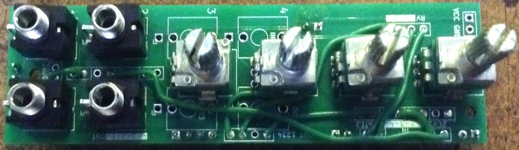
The Pots and Jacks Board
These functions will map onto the following potentiometers and jacks (and connections) from the EuroRack 6HP MCU Pots and Jacks PCB:
| Pot/Jack | Function | Connection |
| RV1 | Potentiometer 1 | GATE 1 |
| RV2 | Potentiometer 2 | GATE 2 |
| RV3 | Potentiometer 3 | OUT 3 |
| RV4 | Potentiometer 4 | OUT 4 |
| IN1 | V/Octave CV IN | OUT 1 |
| IN2 | CV 1 IN | CV 1 |
| IN3 | Not used | |
| IN4 | Not used | |
| OUT1 | Audio OUT | PWM 1 |
| OUT2 | CV 2 IN | CV 2 |
| OUT3 | Not used | |
| OUT4 | Not used |
The pots and jacks PCB should be wired up to the interconnecting headers as follows:
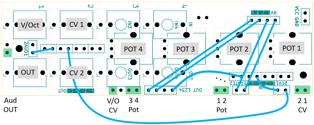
Optionally, it might be useful to connect from the GND header pin to the panel once fitted.
It is suggested the Jacks and Pots PCB is built in the following order:
- Small header pins on the underside of the board.
- Long header pins (if used) on the underside of the board.
- Jacks.
- Potentiometers.
- Link wires.
The Panel
This is the panel design required.
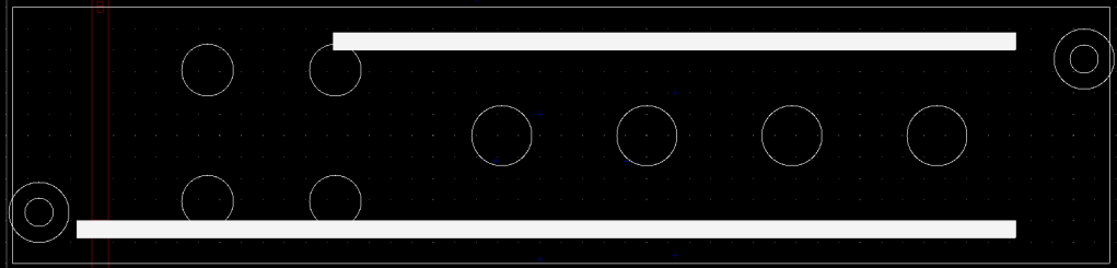
The measurements are all detailed in the EuroRack 6HP MCU Pots and Jacks PCB Build Guide, but crucially the pot holes are M7 and the jack holes are M6. I found they needed a 7.5mm and 6.5mm drill respectively to allow for a bit of flex when fitting the panel.
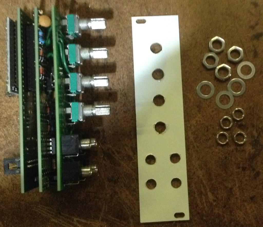
I’ve used M2 mounting posts, screws and nuts between the boards. In particularly, I found that the spacing required a 6mm spacer with an additional nut added as shown below.
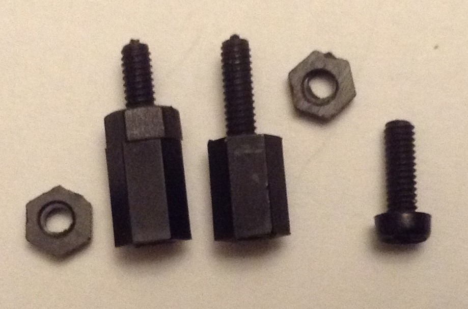
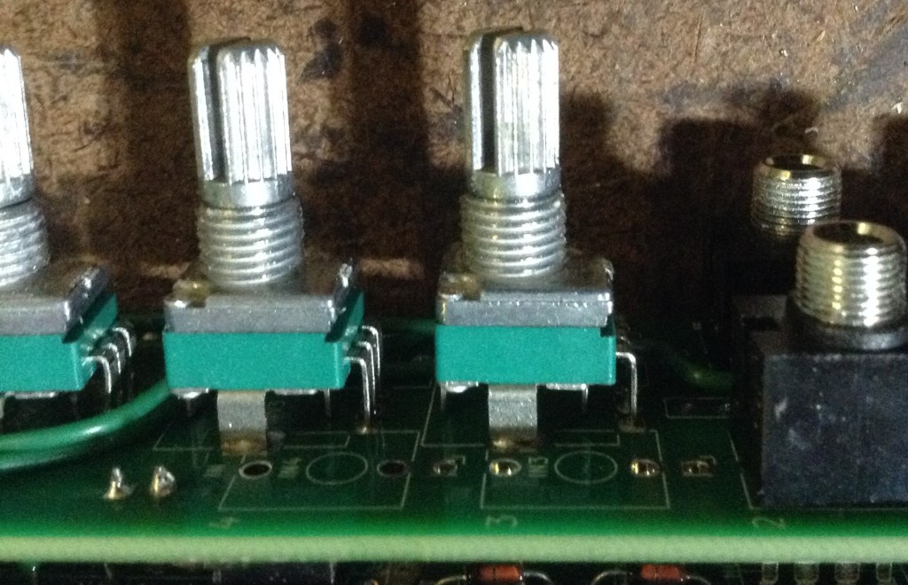
I also had to break off the alignment lugs on the potentiometers to allow the panel to fit snugly.
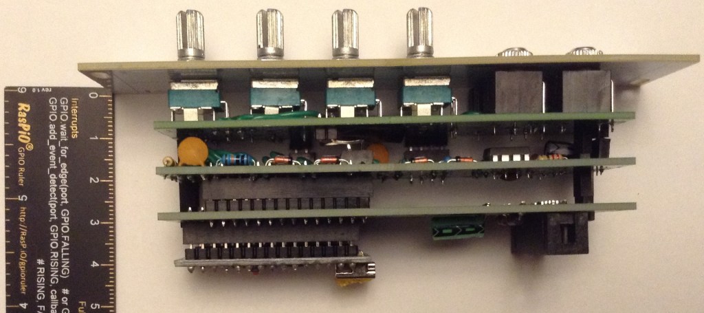
Once all together, you can see it needs around 45 to 50 mm clearance behind the panel for the whole thing.
Testing and Basic Code
I recommend performing the general tests described here: PCBs.
Then it can be connected to an Arduino Nano MCU board an a basic analogRead test can be performed to check the pots and input jacks.
void setup() {
  Serial.begin(9600);
}

void loop() {
  for (int i=0; i<8; i++) {
    int aval = analogRead(A0+i);
    Serial.print(aval);
    Serial.print("\t");
  }
  Serial.print("\n");
  delay(100);
}
An external potentiometer can be connected to a mono patch lead (GND and signal) and VCC to test the CV IN jacks (IN1, IN2, OUT2).
The order should be as follows:
| A0 | IN 1 (1V/Oct) |
| A1 | Not used, floating |
| A2 | POT 3 |
| A3 | POT 4 |
| A4 | POT 1 |
| A5 | POT 2 |
| A6 | IN 2 (CV1) |
| A7 | OUT 2 (CV2) |
The (dual) PWM output can be tested using the basic Mozzi “Hi-Fi” sinewave test which can be found in the examples here:
- Examples -> Mozzi -> 01.Basics -> Sinewave_HIFI
Sample Applications
Here are other posts describing some sample applications for this module.
Closing Thoughts
I have to be honest – working out which parts of the circuits to use, then referring back to them to populate the PCBs, then soldering on the intra-board links and finally fiddling with the panel was actually quite a lot of work.
I don’t know if I’ve saved anything compared to just building the circuit from scratch on a piece of protoboard.
It is also going to be quite likely that any issues might be hard to trace too.
I might find that as I use more of these boards, (assuming I build some more of course), then I get to know the layout and circuits and won’t be referring back to the designs so much. I’ll have to see how it goes.
But for now, if all you want is a single Arduino Nano HAGIWO circuit, then you’re probably better off just making it up on protoboard…
But I think the whole board “sandwich” once complete does look pretty good!
I’ll have to see if I can get a bit of a “production line” going and make up a few more. And now I have to get on with some code…
Kevin

Hi Kevin, this is such a useful series of PCBs! I’ve got up set of the Daisy and MCU control boards, I/O and pots/jacks boards and am in the process of populating the boards. One very general question – assuming a Daisy Seed, would I use the I/O board connections to link to pots/jacks board as shown here for an Arduino Nano?: https://diyelectromusic.com/2025/01/05/eurorack-6hp-arduino-mozzi-module-basic-vco/
Essentially I’m wondering if I need to connect the gates, C/V/ pots and audio any differently with a Seed and the I/O board vs a Nano/ – it looks as though all the necessary connections are fed through the boards as is, but wanted to check. I hope you’re still geting time to work on new ideas, I’m really grateful for all your work
LikeLike
I believe it should all be ok. I have to confess I’ve not done very much with these boards since designing them. I found the re-routing of everything was actually pretty tricky to do in the end, so think it would be a lot easier to have some preset pot/jack configurations to reduce mistakes and the number of wires required for soldering.
But I don’t see why it shouldn’t all work. The Daisy IO I believe is 3V3, so it will require values more similar to those required for using a Pico, which are probably different to the control board values used for the Nano. The board was meant to provide some kind of generic routed board for HAGIWO type modules, so all component selections should be listed in the tables that let to the design of the IO board in the first place. As I say, I’m not sure its really made things much easier. I’ve certainly not built any proper 3V3 logic modules myself for it yet.
Please do take significant note of my warnings though. A mistake on this could take out the power supply of a EuroRack and if real modules are plugged in could cause many £100s of damage to those too…
This is really just a “messing around” module for me, so it really hasn’t had much proper use.
I really ought to do a proper Daisy Eurorack module at some point, but I keep getting distracted 🙂
Good luck!
Kevin
LikeLike