At the end of part 1, I’ve established that the basics all seem ok (PCB, interconnections, power) and that basic digital logic stuff is happening.
In part 2 I checked the ROM, reflowed a number of the solder joints, and started to look at the connectors between the main PCB and the LCD, but still with no luck.
Now I’m finally getting around to looking properly at those data signals to see what my next steps might be.
Oh and nope, still not fixed. Sorry.
Warning! I am not an electronics person. I strongly recommend that you don’t base your own attempts at fixing a beloved vintage synth on anything I’ve said here. I was given this synth rather than it being sent it to a recycling centre so this is a low-risk learning activity for me. I am not responsible for any damage to expensive or irreplaceable electronic musical instruments! There are plenty of places to take something for a proper repair 🙂
If you are new to microcontrollers and electronics, see the Getting Started pages.
Replacing the LCD – Continued
In part 2 I thought that it would be worth seeing if I could replace the LCD with an alternative, seeing as it appeared to be just a common HD44780 based display, but the connector used was giving me trouble.
In the end I just took the plastic shrouds off some Dupont style jumper wires and poked them directly into the connector on the PCB.
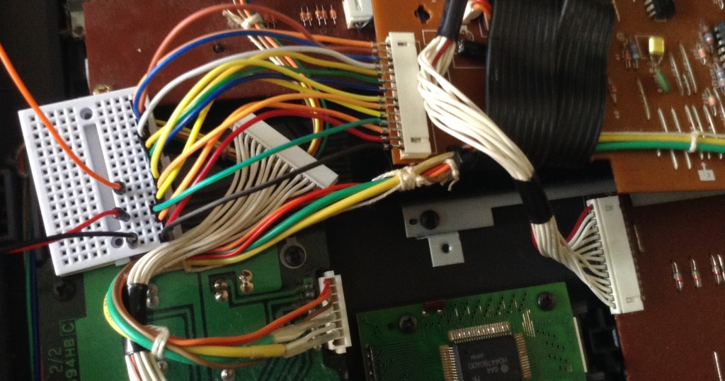
This finally gives me a way into some of the control signals and data lines on the main bus. First things first, I connected up a replacement display. Usefully the pinout of this connector matches exactly the pinout of a LCD1602 display.

The only additional connections required are an extra +5V/GND for the backlight (marked as “K” and “A” on my display). All the other connections match as shown by the schematic.

Hooking up an oscilloscope as follows:
- Yellow = E = LCD Enable pin (decoded from A10-15=0; A13=1)
- Blue = R/W (low = write)
- Purple = RS = register select (maps onto A0 on the address bus)
- Darker blue = D0
and triggering off the enable pin gives me the following trace:
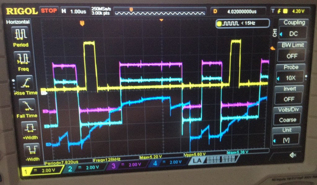
The darker blue line is D0 and as can be seen – it is basically all over the place. It definitely looks like something is breaking the data lines, so the question now is what. I also checked D1-D7 and they all look pretty similar.
From my previous experiments the fact that I can read the ROM successfully, and now have replaced the LCD implies one of the other devices. So I think that leaves the following options:
- The CPU itself
- RAM
- A/D
- OPP – the Yamaha FM tone generator itself
But as all these are soldered down, it makes the next step a little tricky.
I’ve triggered the scope of the various CS/OE lines for the RAM, ADC and OPP and checked the local equivalent of D0 and the pattern seems the same everywhere.
Interestingly I don’t ever see a CS/OE line for the ADC or OPP – but then if it is failing to boot then the CPU will never get around to trying to access either of those I’d imagine.
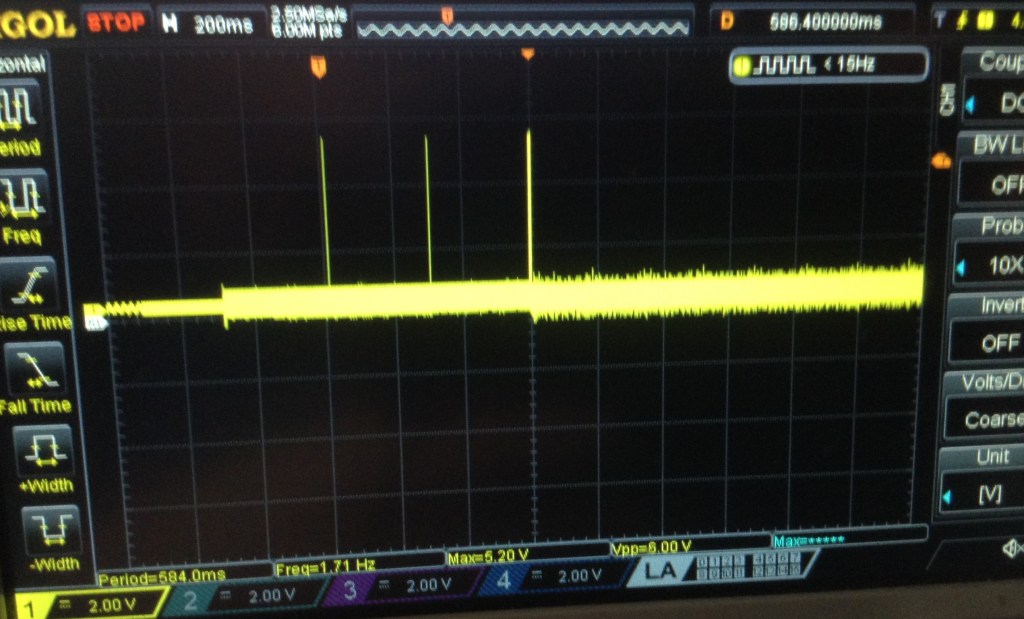
By the way, on startup, there are there points where the LCD “E”nable pin is accessed. Two single instances, and then a large block as shown below.
Removing the ROM
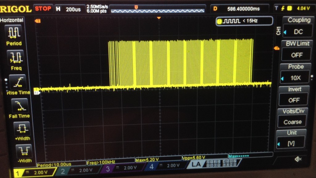
Just out of interest I thought it was worth seeing what the signals looked like with the ROM removed (seeing as it is socketed and easy to remove). I triggered of the CE for one of the RAM chips and checked the signals.
The RAM isn’t accessed as much, but then with no ROM I don’t know what the CPU would be doing anyway…
But when it is, D0 (dark blue again in the trace below) looks a lot more like a sensible digital signal to me.

So now I’m thinking I really ought to eliminate the idea of a problem ROM chip before desoldering any of the RAM to test that…
Aside: at one point, when just monitoring the data signal, I got a much cleaner signal, but very definitely appearing to show three distinct states, which again reinforces the fact that something, somewhere is trashing over the data lines…

Replacing the ROM
As discussed last time, the DX100 uses a 27C256 style ROM which isn’t quite the same pinout as the more common 28C256 EEPROM that can be found relatively easily these days. However there is also a 29C256 which does have essentially the same pinout as the 27C256.
I happen to have some, but I don’t know if they are any good! I also have my Arduino EEPROM Reader but I’ve never tried to write with it and certainly not tried to do anything with a 29C256.
I took the plunge and bought myself an XGecu T48. Downloading and installing the software was a bit of a leap of (hopefully not misplaced) faith as some of download links went off to a media file download site which was constantly playing “download button roulette” but with a bit of care I was able to find the .rar file for the installer.
I programed an Atmel 29C256 with the binary image I found, but unfortunately it made no difference – it was still completely dead.
Just out of interest I tried to read the Yamaha ROM using the XGecu, but I couldn’t find a manufacturers 27C256 setting that worked. I kept getting a “pin 1 error” whenever I tried to read it. Funny that it worked ok with my Arduino reader though…
I tried it with the replacement LED but then plugged the real one back in – but still nothing unfortunately.
One Last Probe…
I thought I’d have one last poke about for continuity with a multimeter. I checked the ribbons that connected different parts of the PCB together. I checked a whole range of GND connections (the additional, unpopulated header in the top right (from the underside) for E, +5, -3 was really useful there.
One oddity I did find, is that I couldn’t find continuity between the VCC pin on one of the RAM chips – IC13. I tried tracing it through to see where things broke, and it got a bit confusing linking into some transistors and eventually the on-PCB battery.
It turns out, looking at the schematic, that this is the RAM battery-backup store:
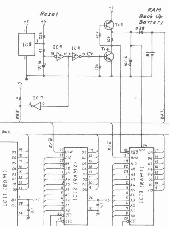
So I guess that means that RAM1 is for voice data and RAM2 is working RAM for the CPU. Curiously, /CE2 for RAM1 is connected into the battery or reset (or both) circuit somehow too, whereas for RAM2 it is tied to GND. I must confess I’m not quite sure what is going on there.
Ah, turns out I should just RTF(service)M. Wiring /CE2 into the reset circuit like this ensures that RAM1 can’t be selected during the reset period and so inadvertently get written to, to override the stored contents. RAM1 is thus disabled until the reset is complete.
/CE1 for both chips is connected to IC14 which does the address decoding (see Part 1).
Anyway the upshot of all this is that I powered the thing back up to check the VCC signals and yes, both pin 24s on both RAM chips are reading 4.99V and the battery itself is reading ~2.5V.
Further Thoughts
I feel like I’ve made a little more progress in appearing to have eliminated the LCD and probably the ROM as a source of the issue.
But I think I’m essentially out of options now. Assuming (and this might be a big assumption of course) everything I’ve said so far is true, I think this only leaves one of the soldered chips as possibly causing an issue. For that, I have the choice of:
- The main application processor itself.
- The two RAM chips.
- The Yamaha YM sound processor.
I think at this point ideally I get some traces from a working synth to see how it compares before desoldering chips. But that probably isn’t going to be possible. Another option might be to look out for a “spares or repairs” DX100 so I can do some mixing and matching.
It might be worth replacing the ROM with hard-wired pull-ups/downs on the data lines to force the code for a NOP onto the bus as the CPU starts up. That at least might show that the CPU itself is still ok. But really, if something is messing with the data lines, the only option really is to remove some of the chips until they start looking sensible again.
But I’m not sure I’m confident enough in my diagnosis so far to start getting destructive so I suspect this might be the end of my journey attempting this myself and I might have to find someone who knows what they are doing.
Of course, if you spot any other options do feel free to let me know.
Kevin

@diyelectromusic.com hard to say whats wrong from your scope picture as the signals aren't labeled. That one signal going all over the place looks horrible but the rest seems to indicate a cpu that is at least partially running.
LikeLiked by 1 person
Remote Reply
Original Comment URL
Your Profile
Why do I need to enter my profile?
This site is part of the ⁂ open social web, a network of interconnected social platforms (like Mastodon, Pixelfed, Friendica, and others). Unlike centralized social media, your account lives on a platform of your choice, and you can interact with people across different platforms.
By entering your profile, we can send you to your account where you can complete this action.
@diyelectromusic.com I'd also think a busted ADC or synth chip wouldn't keep the display from working unless it's clamping down the bus.
LikeLiked by 1 person
Remote Reply
Original Comment URL
Your Profile
Why do I need to enter my profile?
This site is part of the ⁂ open social web, a network of interconnected social platforms (like Mastodon, Pixelfed, Friendica, and others). Unlike centralized social media, your account lives on a platform of your choice, and you can interact with people across different platforms.
By entering your profile, we can send you to your account where you can complete this action.
Yes, the address, clock, CS/CE type signals all seem fine as far as I can see, I think it is just the data lines that are a mess.
Thanks for your comments. I’m still chewing over options! 🙂
Kevin
LikeLike
Kevin, Some observations:
https://github.com/Gustavomurta/Arduino_Mega_Programmer
LikeLike