Before building my Educational DIY Synth Thing I was playing with the ESP32 WROOM dev boards I’d found and was thinking about doing some Mozzi experiments. This post started to document some of the things I’d found out about the boards, but never made it to a complete post.
I’ve now gone back and finished off the design for an experimenter pcb using the dev boards to allow me to do some more playing around with Mozzi and synthesis.
Warning! I strongly recommend using old or second hand equipment for your experiments. I am not responsible for any damage to expensive instruments!
If you are new to microcontrollers, see the Getting Started pages.
Background Information
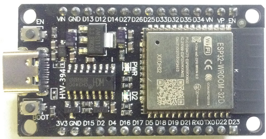
I’m using an entire ESP32 WROOM 32-D DevKit (as shown above) and not just the module itself. This isn’t the official DevKit (note the VIN/3V3/GND pins are different I believe) but it is widely available.
Using the DevKit means I get a few extras “for free”, namely:
- Onboard voltage regulation to 3V3 via a NCP1117.
- USB serial interface via a CH340.
- Reset (EN) and Boot buttons.
- Onboard LED on D2.
- Normal pin headers including extra pins for additional GND connections and VIN.
- USB C connector.
Power Supply
Power is provided via USB or VIN. According to the schematics I’ve found online (which seem to agree with what I can trace out on my board) the power circuit is as follows:

I’ve found some discrepancy in the capacitors values – another schematic suggests C1 here is 100nF. I also found one schematic that shows VCCUSB connected directly to VIN on the NCP1117 rather than via a diode, but my board seems to match the above.
Taking VIN on the module pinout as being the input to the NCP1117 and with a maximum dropout voltage of 1.2V (as per the NCP1117 spec) then the input range for VIN should be 4.5V up to 20V.
As already mentioned, there is an officially documented Espressif ESP32 DevKit (details here and here) but the pinout for this is different to the modules I’ve found that seem pretty common online.
Audio Output
In an effort to keep things relatively simple, I’m keeping with the on-board (internal) DAC of the ESP32. Marcel Licence has a great video (“ESP32 synthesizer with NODAC”) showing how to hook up the two internal DAC channels to an external line out, so I’m going with essentially the same design here.
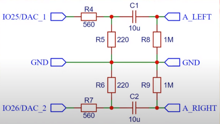
From Marcel’s video:
- “The max voltage of 3.3V will be reduced by the voltage divider (R4+R5, R6+R7)”
- C1 and C2 remove the DC bias as usual.
- “R8, R9 are not really necessary but I added them to avoid an open output when the ESP32 is powered down”.
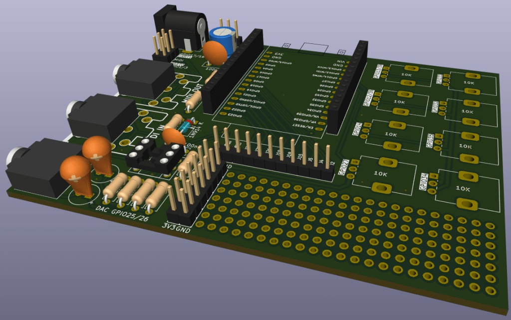
The Circuit

The PCB will support the following:
- 8 potentiometer inputs.
- Audio out from the two DAC channels.
- MIDI IN and OUT (selectable UART 0 or 1).
- Small prototyping area.
- Direct power in (5-12V) to the on-board regulator.
I’ve used Marcel’s DAC output circuit but omitted R8, R9 and adjusted the values of R4, R5 to keep the same ratio for the divider but with slightly adjusted values:
- 220 / (220+560) ~= 0.28
- 1K / (1K + 2K) ~= 0.33
So a 0 to 3.3V signal becomes +/- 550mV.
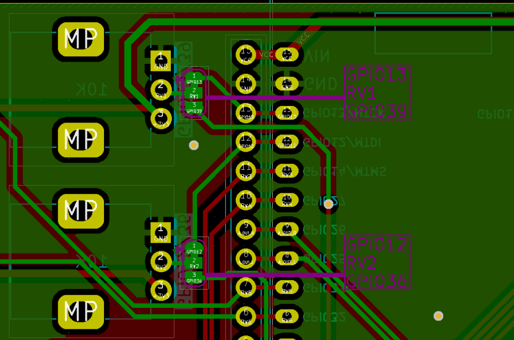
One thing I wasn’t sure about was the use of the strapping pins, so I’ve included solder bridge options to allow the re-patching (or even disconnecting) of two of the pots if required.
The pin mapping used is as follows:
| 2 | GPIO36 / ADC1_CH0 | RV2 option |
| 3 | GPIO39 / ADC1_CH3 | RV1 option |
| 4 | GPIO34 / ADC1_CH6 | RV8 |
| 5 | GPIO35 / ADC1_CH7 | RV7 |
| 6 | GPIO32 / ADC1_CH4 | RV6 |
| 7 | GPIO33 / ADC1_CH5 | RV5 |
| 8 | GPIO25 / DAC 1 | Audio Output |
| 9 | GPIO26 / DAC 2 | Audio Output |
| 10 | GPIO27 / ADC2_CH7 | RV4 |
| 11 | GPIO14 / ADC2_CH6 | RV3 |
| 12 | GPIO12 / ADC2_CH5 | RV2 default |
| 13 | GPIO13 / ADC2_CH4 | RV1 default |
| 21 | GPIO16 / UART1 RX | MIDI IN option |
| 22 | GPIO17 / UART1 TX | MIDI OUT option |
| 27 | GPIO3 / UART0 RX | MIDI IN option |
| 28 | GPIO1 / UART0 TX | MIDI OUT option |
All non-used GPIO pins will also be broken out to additional prototyping headers.
PCB Design

The PCB includes additional header pin connections for all pins of the DevKit and also breaks out the unused GPIO pins to a header row near the prototyping area. There is also a row of 3V3 and GND next to the prototyping area.
I’ve used solder jumpers on the underside of the board to change the GPIO option for RV1 and RV2.
There is also a jumper header to allow the selection of UART 0 or UART 1 for the MIDI links and MIDI supports either TRS or DIN sockets.
There is a stereo TRS for audio output connected to the two DAC outputs. With hindsight, I should have allowed a jumper option for a single DAC to drive both audio channels, but that could be easily supported with an additional jumper wire.

Closing Thoughts
Whilst a bit late for my main experiments with the ESP32, there are still plenty of things I’d like to do with them, and I’ve really not done very much with Mozzi itself, so I think this will end up being really quite handy.
Kevin

Just got my boards back from JLCPCB. I’ll let you know how the build goes
LikeLike
Great! Fingers crossed they work ok for you. 🙂
(Note the point about Mozzi currently seemingly being broken for ESP32! Hopefully that will be sorted soon).
Kevin
LikeLike