One (other) thing I was toying with experimenting with is the whole world of DIY guitar pedals. I don’t know much about them but wanted a platform I could use for experimentation.
- Part 1 – PCB Design and Introduction.
- Part 2 – PCB Build Guide.
- Part 3 – Proto Pedal Usage and Application Notes.
I was intrigued by the Electro-smash DIY pedals based around various Arduino boards or a Raspberry Pi Pico, but they don’t seem to be available anymore and the support forums seem to have dried up.
But as the designs are all open source, I was able to take a look at the design and function and get an idea of what I might want myself. Unfortunately the full open hardware design files are not available on Github (anymore?) but there are quite a few details still on their website about the designs and design process.
So this is my attempt at a prototyping platform for guitar pedals that could support design with either a microcontroller or analog circuits. I’ve found many archives of schematics online and I want a platform that will help me try some of them out.
This might be a one-off – I don’t know yet if this is something I plan to do more of – there is so much to try and learn about (see some of the references below).
Warning! I strongly recommend using old or second hand equipment for your experiments. I am not responsible for any damage to expensive instruments!
Here are some references for DIY guitar pedals:
- https://www.diystompboxes.com/ – and a large list of schematics
- https://www.freestompboxes.org/
- https://stompboxschematics.com/
And some suppliers of DIY kits in the UK (I’ve no experience of these, they are just some examples from browsing around):
- Pete’s DIY Guitar Effects Pedals and the Ultimate Beginner’s Guide
- Jed’s Peds
- Fuzz Dog’s Pedal Parts
If you are new to electronics, see the Getting Started pages.
Introduction / Key Requirements
I want something that can achieve the following:
- Includes pre-amp and post-processing circuitry to support use of microcontrollers at 3V3 or 5V levels (I’m basing this on the fact the Electro-smash pedals include them).
- Includes a prototyping area and easy to use with solderless breadboards.
- Includes the IN and OUT standard (1/4″) mono jacks.
- Has a stomp-switch with a “true bypass” function.
- Can fit in a common pedal enclosure (e.g. the Hammond 1590BB).
- PCB within the 100x100mm cheap limit for PCB manufacturing.
- Includes a 2.1mm barrel jack for power.
- Mounting holes, especially to support the stomp-switch.
Things that would be nice:
- Optional smaller variant for use with smaller enclosures (e.g. the Hammond 1590B).
- Optional – pre mounted, ready to use, potentiometers and switches.
- Easy way to make a solderless breadboard circuit permanent.
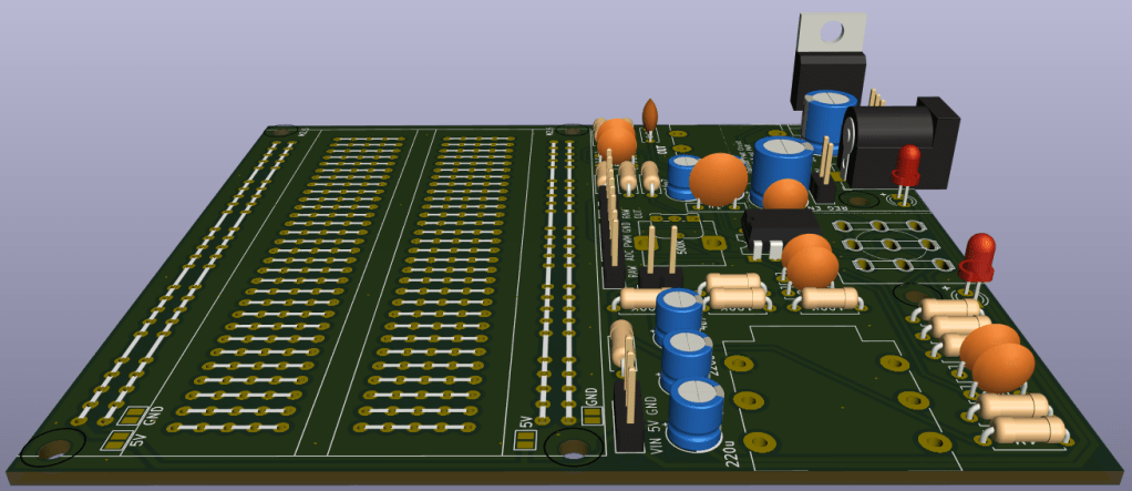
The idea is to design a PCB that has space for mounting a solderless breadboard but also the holes and prototyping area that matches the solderless breadboard layout to make it easy to turn a design into a soldered version.
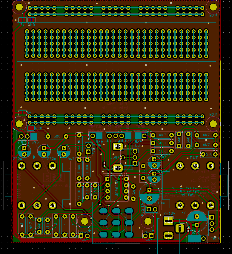
The Circuit
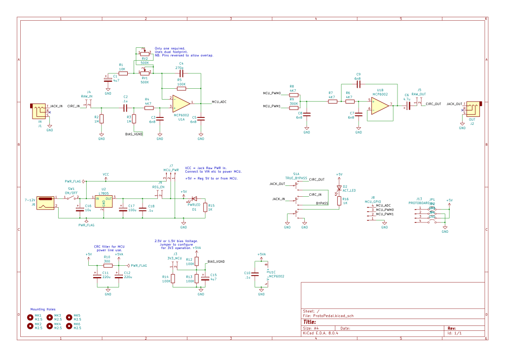
The input and output stages are largely taken from the Electro-smash discussion of their own designs. The MCP6002 is a rail-to-rail opamp and will be running at 5V.
Note that the PWM implementation is a twin-PWM output solution. There is a detailed tutorial on how this works at Open Music Labs. Key to this working correctly is an accurate ratio of those two resistors (4K7 and 300K). Consequently I’ll be using 1% tolerance resistors for these. The filter stage is designed to work with a 5KHz cut-off frequency.
I’ve included a “true bypass” stomp switch. There are loads of references out there for how to wire up the 3-pole, double-throw (3PDT) switch to support this, including an LED to show when the effect is active. I can’t remember exactly which site I used in the end, but the variant I wanted to end up with is as follows:
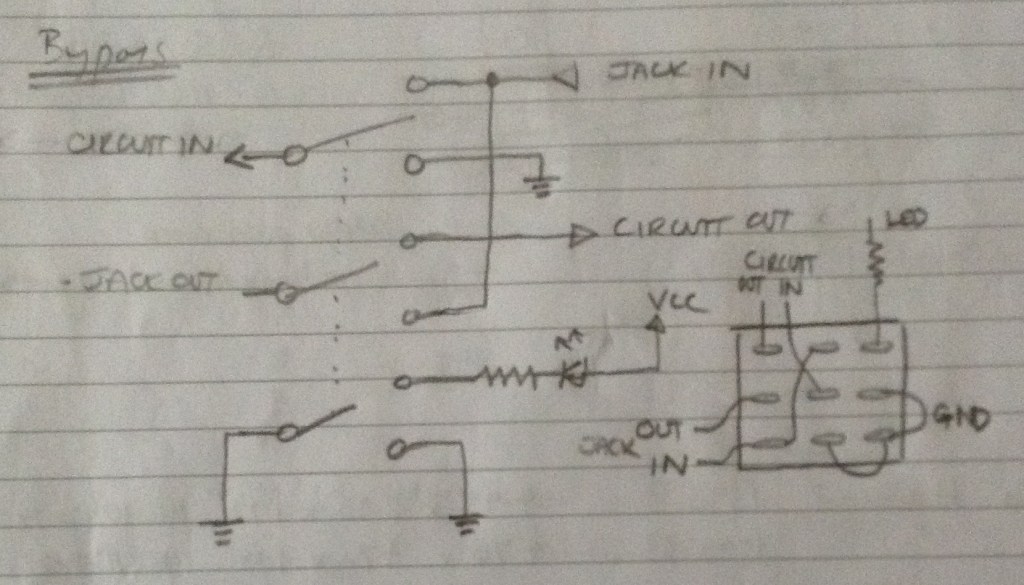
But for some reason (getting interrupted at a crucial moment I expect) I ended up with a slightly simpler version (see schematic). The downside of the simpler version is that the “circuit in” isn’t automatically grounded when inactive. I’ll have to wait and see if that becomes an issue or not…
It appears fixable with a few cut traces and a couple of patch wires though if so.
In terms of power, I wanted to support various options. Ideally:
- The option for power from a 2.1mm barrel jack – so I’ve included a L7805 regulator.
- During prototyping, if using a microcontroller, then the option for power from the microcontroller’s USB port.
I’ve ended up with two jumpers:
- A bias jumper. The input opamp circuit needs a bias voltage that is half of the MCUs expected ADC voltage. There is a jumper to patch in an additional resistor to set the bias voltage to either 2.5V or 1.5V for the case of a 5V or 3.3V MCU, even though the opamp itself is always powered from 5V.
- A MCU/regulator jumper. There is the option to power the whole circuit from either a MCU’s 5V output (even a 3V3 MCU with USB usually has an option for 5V out) or from the regulator on the PCB.
There are additional header points to support connections to the MCU ADC input and PWM outputs, including an extra GND connection.
There are also solder headers to allow for 5V and GND to be patched into the prototyping area if required. These aren’t always enabled as in some circuits these rails might be used for other purposes or a non-5V power rail.
Finally, it is also possible to receive the raw signal input and patch directly to a raw signal output bypassing the opamp circuitry if required.
PCB Design
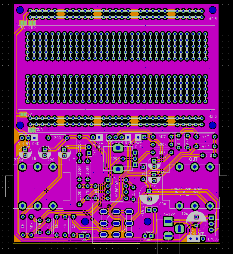
This board required two custom footprints. There is a 3PDT switch footprint in a library provided by Sparkfun but it didn’t look like the through holes were big enough or the right shape for my switches. Consequently I turned the holes into ovals as can be seen above.
I also couldn’t find anything that approximated a solderless breadboard layout for my prototyping area, so I created a footprint for the entire layout. The issue I had was how to create the tracks between holes. In the end I used elongated SMT pads on the same nets.
One downside of this that I hadn’t considered until the boards came back – SMT pads include a footprint in the solder mask layer, so my copper connections between pads are not covered in mask. That is something I can fix in a future footprint revision.
I did manage to get everything within a 100mmx100mm PCB size though, including mounting holes, so I was pretty pleased about that. I positioned two mounting holes either side of the stomp switch to support it, but really most of the pressure on the switch ought to be taken up by a sturdy case.
It was a challenge to be able to include all the jumpers in useful positions for ease of access to the breadboard area. The one compromise is that the power jumper is part selector and part jumper header. There might be a tendency to assume the jumper part is an “either or” – but if the jumper is swapped from one side to the other, then it will end up shorting 5V to GND.
This isn’t ideal, and leaves the potential for user error relatively high, but I couldn’t fit everything in any other way.
I’ve added a number of notes for the power options especially on the silkscreen on the rear of the board.
The power switch has a three-pin, 2.54mm footprint and there is always the option for mounting some of the connectors, LEDs, and switches directly to a case and connected back to the PCB using wires. I anticipated the LEDs would probably be bent over anyway to appear from the bottom of any box, next to the power socket and on/off switch.
One last thing to note – the two standard 1/4″ jack sockets are stereo sockets as they were more readily available, but the “ring” is not used – just the tip and screen. This means they are essentially mono sockets and will accept a standard guitar mono jack lead.
Closing Thoughts
This is a learning project right from the outset so it’s no wonder there are already a few issues to consider for next time.
If I was more disciplined, I’d do this write-up before sending off a PCB to be made, as it acts as quite a significant “design review” stage. It is almost as if actually designing the thing properly up front has some uses 🙂
But once a PCB seems “done” I’m doing well if I manage to leave it overnight before sending it off! Although I do try to stick to that rule if I can.
And finally a bit thank you to Electro-smash for (at least initially) publishing their open hardware designs for their PedalShield and PedalPi.
Kevin
