The 40-pin AY-3-8910 devices I’ve been playing with are no longer newly available, but they are pretty available if you are happy with a certain questionable quality (more on that here: Arduino and AY-3-8910).
But the slightly shorter version (with fewer general purpose I/O pins), the 28 pin AY-3-8912, seems a lot harder to find, despite being widely used at the time. At least, to find on its own – i.e. not already soldered onto a circuit board. There is apparently also an even smaller AY-3-8913 in 24-pin format and a few other lesser used options too. But the 8912 is the variant most often found in the ZX Spectrum 128, Amstrad CPC, and many home computers from the time.
A key modern option then is emulation and there is a very capable AVR emulation of the sound generator online including some on PCBs that directly fit within the 28-pin footprint of the original.
One is Yevgeniy-Olexandrenko’s avr-ay-board for the AY-3-8910, AY-3-8912 and YM2149F devices, with a 8912-compatible DIP-28 PCB design using an ATMega48.
Another is published on https://www.avray.ru/, but that appears to be the firmware only. There is a board that uses this firmware built for an ATMega8P here and another for a two-device (dual AY-3-8912 for 6 channel support is often called “Turbosound”) here.
I don’t believe either of these approaches emulate the general purpose IO pins of the 8912/8910, which might be an issue using them “as is” in a retro system. I know the ZX spectrum 128 uses the IO for example.
Some options for replacing original AY-3-8912 devices:
- vRetro’s AY-3-8912 replacement available from https://www.vretrodesign.com/. There is an option for the original plus a “Turbosound” (6 channel) version.
- Note this includes full IO support so really is a drop-in replacement for use in retro systems (my Harlequin 128K kit came with one for example). The chip I have uses the ATTiny1627 and ATTiny1614. I don’t believe the designs are open (that I’ve found). Curiously these two devices have a max clock of 20MHz (relevant later).
- Adaptor boards to allow use of an AY-3-8910 40-pin device in the AY-3-8912 28-pin footprint, e.g.: https://github.com/etomuc/CPC-AY-3-8910-to-8912-adapter
- RC2014 also provides a board for RC2014 systems using the emulator design from https://www.avray.ru/ in place of an original AY-3-8910: https://rc2014.co.uk/modules/why-em-ulator-sound-module/. This uses an ATMega48PA running at 27MHz (see schematic).
- At least one FPGA based replacement: https://retrolemon.co.uk/sinclair/256-ayfpga-dual-ay-turbosound.html
But perhaps my favourite so far is the slightly random, “building an AY-3-8910 out of discrete logic” that I must have a proper look at, at some point: https://github.com/mengstr/Discrete-AY-3-8910
This post looks at how AVR emulation of AY devices works in a little more detail and maybe take some starter steps to reproduce my own.
Warning! I strongly recommend using old or second hand equipment for your experiments. I am not responsible for any damage to expensive instruments!
If you are new to microcontrollers, see the Getting Started pages.
AVR-AY-Board
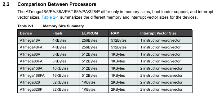
The avr-ay-board is a fully open source design and can use an ATMega48, 88, 168 or 328. The ATMega328P is very commonly used on an Arduino Uno or Nano.
Full details, including a schematic, gerber files, BOM, and firmware are available here: https://github.com/Yevgeniy-Olexandrenko/avr-ay-board.
It shares a lot of firmware heritage with the source available from https://www.avray.ru/. Up until Feb this year there was a link back to the original source, but that has since been removed and it appears to have mostly diverged some time in 2022. There is a list of differences here, but much of the discussion that follows would probably apply to both versions of the code.
The only difference between the ATMega48, 88, 168 and 328 is the amount of memory. They are named for the amount of flash memory – 4K, 8K, 16K, 32K respectively. But otherwise they are functionally identical. Here is the key data from the datasheet:
Note that the ATMega328PB is an enhanced version of the ATMega328P which itself is a slightly lower power (as I understand things) version of the original ATMega328. Application note “AT15007: Differences between ATmega328/P and ATmega328PB” lists the full set of enhancements, but it includes additional UART, SPI, I2C, and timers, although it is essentially backwards compatible with the 328/328P.
All of this means that a standard Arduino Uno or Nano might be able to run the bespoke AY-3-8912 emulation firmware and with the appropriate pin connections might also be able to emulate an AY-3-8912 in another system. Naturally it will be physically larger than the original chip, but electrically it should all work fine.
The Circuit
The original ABR-AY-Board is relatively straight forward. The full schematic is available in the GitHub repository and shows the following:
- A minimal ATTMega48P support circuit (capacitors, oscillator, power, LED).
- Three low-pass filters to filter PWM to an audio output expecting a 1K load (apparently).
- A mapping onto the AY-3-8912 28-pin pinout.
There used to be a detailed “usage” section on the GitHub but that has since been removed, but from the published schematic (v1.5) the pins are accessed and mapped as follows.
| AY-3-8912 | Schematic | ATMega48P | Arduino Equivalent |
| D0-D5 | D0-D5 | PC0-PC5 | A0-A5 |
| D6-D7 | D6-D7 | PD6-PD7 | D6-D7 |
| A8 | MISO_A8 | PB4 | D12 |
| BC1 | BC1 | PD2 | D2 |
| BC2 | SCK | PB5 | D13 |
| BDIR | BDIR | PD3 | D3 |
| CLOCK | CLOCK | PD4 | D4 |
| RESET | RESET | PC6 | RESET |
| TEST | MOSI_PWM_B | PB3 | D11 |
| IOA7-IOA0 | N/C | ||
| C | OUT_C / PWM_C | PB2 | D10 |
| B | OUT_B / MOSI_PWM_B | PB3 | D11 |
| A | OUT_A / PWM_A | PB1 | D9 |
| CFG0 | PB0 | D8 | |
| CFG1 | PD5 | D5 | |
| RX | PD0 | D0 | |
| TX | PD1 | D1 | |
| VCC | VCC | VCC | VCC |
| GND | GND | GND | GND |
There is a UART header (TX, RX, VCC, GND), ICSP header (MISO, MOSI, SCK, RESET, VCC, GND), and two configuration jumpers (CFG0, CFG1).
One point that might cause issues mapping over to an Arduino Uno or Nano is that the avr-ay-board has a 27MHz oscillator, whereas the Arduino only runs at 16MHz. That will almost certainly need some looking at.
The Clocks
So about that 27MHz clock. The default Arduino has a 16MHz oscillator so could this run on an unmodified Arduino?
Looking through the code, there seems to be one specific mention of the CPU frequency:
    ; --------------------------------------------------------------------------
    ; Init Timer0
    ; --------------------------------------------------------------------------

    ; Fast PWM, TOP = OCR0A
    ldi     r16, (1 << WGM01) | (1 << WGM00)
    OutReg  TCCR0A, r16
    ldi     r16, (1 << WGM02) | (1 << CS00);
    OutReg  TCCR0B, r16

    ; 219512 Hz internal update clock
    ;ldi     r16, (27000000 / (1750000 / 8) - 1)
    ;out     OCR0A, r16
    OutReg  EEARL, YH               ; set EEPROM address 2
    sbi     EECR, b0
    InReg   r18, EEDR               ; load byte 2 from EEPROM to r18
    OutReg  OCR0A, r18              ; set PWM speed from byte 2 of EEPROM (affect AY chip frequency)
In the commented out code, there is reference to 27000000. But then that appears to be replaced with code that is reading the PWM frequency from EEPROM.
At the start of the main file is the comment:
; ==============================================================================
; Configuration
; ==============================================================================

; EEPROM Config:
; byte 0 - Serial interface enable (1 - enabled)
; byte 1 - Parallel interface enable (1 - enabled)
; byte 2 - PWM speed depending on AY chip frequency and MCU clock frequency
; byte 3 - USART baud speed depending on MCU clock frequency
In the build area there is the main hex firmware and then three configurations with the following contents:
; firmware/v1.0/compiled/config-1.75mhz.hex
:0500000001017A3AFF46
:00000001FF

; firmware/v1.0/compiled/config-1.78mhz.hex
:050000000101783AFF48
:00000001FF

; firmware/v1.0/compiled/config-2.00mhz.hex
:0500000001016B3AFF55
:00000001FF
We can see these differing in the values after 0500000. The next two bytes (0101) map to serial and parallel interface being enabled. These define how the AY-3-8912 registers can be accessed, either using the original device’s parallel data bus or via a newer serial link. The serial link can be used to send register-value pairs to the device rather than use a real AY compatible parallel bus interface.
Then there is a differing byte (7A, 78, or 6B respectively) which is pulled into the timer 0 frequency code and used to set OCR0A in the previous code.
Finally that last byte of the configuration (3A) relating to USART baud, which I infer from older comments in the README file will be 57600, but this is as yet unverified.
On studying the code, it quickly becomes apparent that the whole execution is optimised for specific MCU clock frequencies. This is particularly notable in the interrupt routines, for example, the following:
; ==============================================================================
; Parallel communication mode (BC1 on PD2/INT0, BDIR on PD3/INT1)
; ==============================================================================
ISR_INT0:                           ; [4] enter interrupt
    sbic    PinD, PD_BDIR           ; [2/1] check BDIR bit, skip next if clear
    rjmp    LATCH_REG_ADDR          ; [0/2]

    ; [ READ MODE ] (BC1=1, BDIR=0)
    ; --------------------------------------------------------------------------
    ; 350ns max to set data bus, 8 cycles to set
    ; 8 * 37ns = 296ns for 27MHz O.K.
    ; 8 * 40ns = 320ns for 25MHz O.K.
    ; 8 * 42ns = 336ns for 24MHz O.K.
    ; 8 * 50ns = 400ns for 20MHz !!!!
    OutReg  DDRC, BusOut1           ; [1] output -> low level on D0-D5
    OutReg  DDRD, BusOut2           ; [1] output -> low level on D6-D7
Here we can see that running at 20MHz (for example) violates the timing constraint to respond with the data on the bus. Running at 24MHz, 25MHz and 27MHz appears to be fine. There are a number of other places in the code where similar comments have been made.
The conclusion seems pretty clear. A standard Arduino Uno or Nano running at 16MHz would not work. Something at 20MHz might do the job with some limits, but there is definitely a reason the board is using 27MHz.
There is a key issue however. AVR 8-bit microcontrollers are typically only specified for up to 20MHz operation. I’ve certainly not found any ATMega48 through to ATMega328 that has a higher frequency specification. There are some newer 8-bit devices that might stretch to 24MHz.
But I’m now wondering if the MCU is being overclocked on this board. It would appear, according to some superficial searching, that people have been overclocking AVRs for years…
Timer Configuration and PWM Output
The emulator is using PWM to produce audio from the AVR. The PWM channels/timers are allocated as follows:
| AVR Pin | Timer Output | Compare Register | Timer | |
| System Clock | D4 / PD4 | N/A | OCR0A | 0 |
| Channel A | D9 / PB1 | OC1A | OCR1AL | 1 |
| Channel B | D11 / PB3 | OC2A | OCR2A | 2 |
| Channel C | D10 / PB2 | OC1B | OCR1BL | 1 |
The first timer, Timer 0, I’ve already mentioned, is used to set the basic internal system “clock” for the emulation. In the real AY PSG the internal clock for tones is set to the external clock / 16 and for envelopes is external clock / 256. In the emulation this is all set in code and the CLOCK input is ignored.
The 8-bit Timer 0 configuration is as follows:
- TCCR0A/TCCR0B = WGM00 | WGM01 | WGM02 | CS00
- OCR0A = value from EEPROM (as mentioned previously)
This uses timer 0 in Fast PWM mode (WGM = 7) with TOP = OCR0A and no prescaler. There is a check in the main loop for Timer 0 overflow which is then used to determine if the sound generation should be processed. This effectively sets the CLOCK for the emulation. The AY CLOCK input is meant to be between 1MHz and 2MHz and EEPROM configurations are provided to emulate 1.75MH, 1.78MHz and 2.0MHz external clocks.
In Fast PWM mode, from the ATMega328 datasheet, for Timer 0, the frequency is given by:
- FreqPWM = FreqCLOCK / (N * 256)
Where N is the prescaler factor, so in this case 1. But this appears to be stated for the case when TOP = 255. If the TOP is reduced, so when TOP = OC0A, then presumably that 256 should be (TOP + 1). Assuming this to be the case, then with a 27MHz clock and the previously mentioned values from the EEPROM, we have
- 0x7A = 122 -> timer freq = 27 MHz / 123 = 219.5 kHz
- 0x78 = 120 -> timer freq = 27 MHz / 121 = 223 kHz
- 0x6B = 107 -> timer freq = 27 MHz / 108 = 250 kHz
These give a basic operating frequency of between 3.5MHz and 4MHz which is twice as fast as the real PSG. I’m guessing that this is because the sound generation code (later) toggles the output value on each period, which therefore requires doubling the frequency to generate the high and low periods.
Note that although this timer is configured in Fast PWM mode, it isn’t actually running PWM, it is just used as a timer. The timer also never “triggers” as such – it is polled for overflow within the main code loop.
The 16-bit Timer 1 configuration:
- TCCR1A/TCCR1B = WGM10 | WGM12 | COM1A1 | COM1B1 | CS10
- PB1 and PB2 set to OUPUT for PWM out on OC1A and OC1B.
This uses timer 1 in 8-bit Fast PWM mode (WGM = 5) with TOP = 0xFF. There is no pre-scaling and OC1A/OC1B cleared on compare match with OC1A/OC1B set at BOTTOM (non-inverting mode).
The 8-bit Timer 2 configuration:
- TCCR2A/TCCR2B = WGM20 | WGM21 | COM2A1 | CS20
- PB3 set to OUTPUT for PWM out on OC2A.
This uses timer 2 in Fast PWM module with TOP = 0xFF (WGM = 3). OC2 is clear on match and set at BOTTOM (non-inverting again).
The PWM resolution for both Timer 1 and Timer 2 will be 8-bits (0 to 255) and the frequency for the output is given by the same formula used for Timer 0, giving a PWM frequency of:
- FreqPWM = 27 MHz / (255+1) = 105.5kHz
Bus Access
There is a comprehensive bus access protocol defined in the AY-3-8910/12 datasheet with several possible modes involving the control signals BC1, BC2, BDIR, and A8 plus /A9 (in the case of the 8910). In particular, there is some redundancy in how the “LATCH” is indicated (see section 2.3 in the “AY-3-8910/8912 Programmable Sound Generator Data Manual” – more here: AY-3-8910 Experimenter PCB Design).
For the emulator, BC1 is tied into the AVR INT0 (via PD2/D2) and BDIR is tied into AVR INT1 (via PD3/D3). If the serial interface is used then there is also an interrupt for the UART. BC2 is ignored so all responses are enacted upon as if BC2 is set to HIGH.:
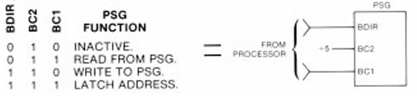
The basic operation, as far as I can see, is as follows:
INT0 ISR - triggered on BC1 -> 1
  IF BDIR == 0  // BC1=1; BDIR=0: Read data
    Set data lines to OUTPUT
    Write BusOut to the data bus
    WAIT for BC1 -> 0
    Set data lines to INPUT

  ELSE BDIR == 1 // BC1; BDIR=1: Latch Address for read
    Read ADDR from data lines
    Grab value from pseudo register in RAM into BusOut

INT1 ISR - triggered on BDIR -> 1
  IF BC1 == 0  // BC1=0; BDIR=1: Write data
    Read DATA from data lines
    Store value to pseudo register in RAM

  ELSE BC1 == 1 // BC1=1; BDIR=1: Latch Address for write
    Read ADDR from data lines
There is a pseudo image of all AY registers stored in RAM which is used by the main loop for the sound processing. This RAM image is updated when the AY is written to and can be accessed when the AY is read.
Note that there is no access control. If an interrupt comes in part way through an update to the sound generators they will stop process and then continue from that point unaware than any register updates have taken place. This does mean that if any registers are accessed twice, it is quite possible that they would have changed by the time of the second access.
Similar logic happens within the UART interrupt handler, but instead address and data values are obtained over the serial port and interactions with RAM updated according to the bytes recieved.
I’ve not looked further into the serial handling at this time other than to note that all updating is performed withing the UART ISR which is receive only.
Main Sound Processing Loop
The main logic free runs as follows:
MAIN Loop:
  IF Timer 0 Overflow Flag is SET:
    Process envelope generator
    Process noise generator
    Process tone generator for channel A
    Process tone generator for channel B
    Process tone generator for channel C
    Process mixer control
    Process amplitude control for channel A
    Process amplitude control for channel B
    Process amplitude control for channel C
    Update PWM values in OCR1AL (ch A), OCR2A (ch B), OCR1BL (ch C)
So the loop essentially pauses until timer 0 overflows at which point all sound generation activity undertakes a single scan and then the PWM sound generation registers are updated.
Before I dive in, I should note that the register definitions are of the form AY_REGnn where nn is a decimal from 00 to 15. The datasheet describes Ro where o is an octal value from R0 to R7, then R10 to R17. I will be using the decimal versions here to match with the code.
I’m not going to work through how the sound generation works in its entirety right now, but I will just include a note about the tone generation. Here is the code for channel A.
    ; Channel A
    subi    CntAL, 0x01             ; CntA - 1
    sbci    CntAH, 0x00
    brpl    CH_A_NO_CHANGE          ; CntA >= 0
    lds     CntAL, AY_REG00         ; update channel A tone period counter
    lds     CntAH, AY_REG01
    subi    CntAL, 0x01             ; CntA - 1
    sbci    CntAH, 0x00
    eor     TNLevel, ZH             ; TNLevel xor 1 (change logical level of channel A)
CH_A_NO_CHANGE:
All counters (CntAL and CntAH for channel A) are 16-bit values. AY_REG00 and AY_REG01 are the RAM copies of the two tone generator registers for channel A.
We can see that the channel counter is decremented on each scan through the routine implementing the following pseudo code:
counter--
IF (counter == 0):
  Reset counter from AY_REG00 and AY_REG01
  Toggle logic level for channel A
This means that the output square wave value for channel A will toggle between HIGH and LOW every time the counter reaches zero and that the counter will have to count to zero twice to make a complete cycle of the square wave.
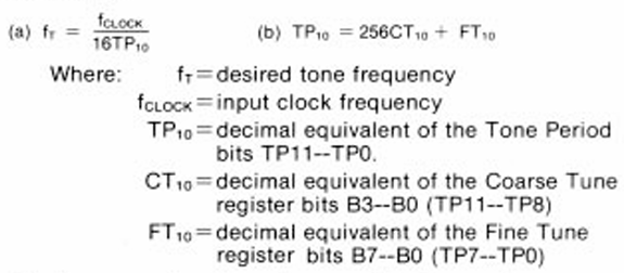
The datasheet states that the tone registers define a 12-bit tone generator period:
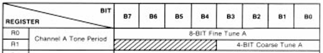
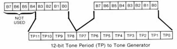
The resulting sound frequency is given by the equation:
As we have to count twice to get our square wave output, we can see why the timer 0 “clock” frequency has to be twice the desired running CLOCK of the AY-3-8912. An alternative implementation could have been to add an additional check as part of the countdown to change the waveform half-way through.
This does mean that all sound generator registers are processed twice as quickly as expected so that might have to be taken into account when calculating other parameters.
The main impact would be for the envelope generator, which according to the data sheet runs a frequency CLOCK / 256. There is a EG period counter defined by AY_REG11 and AY_REG12 (R13 and R14) for further subdivision, so a full sweep of the envelope will happen with a frequency of CLOCK / (256 * EGcounter).
The datasheet also notes that “the envelope generator further counts down the envelope frequency by 16 producing a 16-state per cycle envelope pattern”. This means that the frequency required to process each individual step of these 16 states is: 16 * CLOCK / (256 * EGCounter) or CLOCK / (16 * EGCounter).
The Envelope Code is essentially doing the following:
Every LOOP scan:
  IF env reg updated:
    Reinitialise EG
    Reset EGCounter from AY_REG11, AY_REG12
    EGPeriod = 31
    Re-enable EG

  ELSE
    IF EG enabled:
      EGCounter --
      IF EGCounter == 0:
        EGPeriod --
        IF EGperiod == 0:
          EGPeriod = 31
          Disable EG

        Reset EGCounter from AY_REG11, AY_REG12
        Eval = Envelope value
This implies that a full sweep of the envelope takes EGcounter * 32 scans of the main LOOP. As the LOOP is running at twice the frequency of the CLOCK. this gives an EG frequency of:
- LOOP / (32 * EGcounter) = CLOCK * 2 / (32 * EGCounter) = CLOCK / (16 * EGCounter)
Which matches the datasheet. So the doubling of the LOOP frequency is taken into account by having 32 steps for the EG base period rather than 16.
A few other observations from the code:
- The envelope period counters are stored in AY_REG11 and AY_REG12 (R13 and R14) and managed using CntEL and CntEH via r26 and r27.
- The line ‘sbiw CntEL, 0x01’ is a 16-bit instruction and so acts on both r26 (CntEL) and r27 (CntEH) at the same time as a HIGH/LOW 16-bit pair.
- The counter updating currently happens at the LOOP frequency which is 2 * CLOCK. Every time the counter hits 0 the step is advanced. It therefore takes 32 * counter passes through the LOOP to process the entire cycle of the envelope.
- The envelope period is managed using TabP which is initilised to 0x1F (31 decimal).
- Whenever the envelope counter reaches 0 the next envelope period is selected via TabP.
- The resultant envelope value is stored in Eval which is used as the maximum value for the amplitude calculations later in the loop.
Curiously there are two envelope volume tables provided as options. The first (“AY_TABLE”) distinctly shows the doubling of levels turning 16 values into 32 values. The second (“YM_TABLE”) appears to have some interpolation between values giving a higher resolution envelope.
From wikipedia: “The input clock is first divided by 16 (or by 8 in the YM2149, because the envelope generator has twice as many steps, and thus needs twice as many clocks to complete a full cycle), and then by the 16-bit value.”
So by starting with double the CLOCK frequency, we effectively get YM compatibility “for free”.
Only a single envelope table is required – it defines a linear incrementing pattern that is then used and reused in various ways according to the EG control bits in AY_REG13 (R15) as per figure 7 in the datasheet. I’m not going to dig into that further at this point. I might come back to it in the future.
I’m also not going to dig into the noise generation, mixer or amplitude control at this time.
Closing Thoughts
I really like I feel I know a lot more about how the AY-3-8910/8912 work now and certainly am, as usual, in awe of those who figured all this out and then how to emulate it on a modern (ish) microcontroller.
It is also interesting to note that the emulation hasn’t been updated, as far as I know, for anything more capable than an 8-bit AVR. I guessing it just isn’t necessary and avoiding the whole 3V3/5V logic thing has a certain appeal.
The two commercially available solutions I’ve seen from RC2014 for the WhyEm sound card and the vRetro 28-pin direct replacements, stick with AVR and overclock as far as I can tell. RC2014 using ATMega48AP at 27MHz and vRetro using two ATTiny MCUs and what I think is a 30MHz oscillator.
I would like to see if I can get a standard ATMega328P running the code and then I’d be really interested in seeing if it could be made to run on a Logic Green LGT8F328 “AVR clone” that apparently should be able to run at 32MHz.
I believe I’ve convinced myself not to attempt to build the AY-3-8910 out of discrete logic…
Kevin
