Here are the usage notes for my Proto Pedal PCB Design.
- Part 1 – PCB Design and Introduction.
- Part 2 – PCB Build Guide.
- Part 3 – Proto Pedal Usage and Application Notes.

Warning! I strongly recommend using old or second hand equipment for your experiments. I am not responsible for any damage to expensive instruments!
If you are new to electronics, see the Getting Started pages.
Errata Implementations
These notes are assuming that the jack socket wiring has been corrected.
This is the issue that if the bypass switch is activated with no jack plugged into the OUT socket then the IN signal will be shorted to GND.
Power Supply Jumper Settings
There are two main ways to power the board.
- 7-12V power via 2.1mm barrel jack and on-PCB regulator.
- 5V power from a microcontroller.
There are options to support use with or without a microcontroller, and options for either 5V (e.g. Arduino Nano) or 3V3 (e.g. Raspberry Pi Pico) microcontrollers.
Here are the required jumper settings for the various options (yellow box filled = jumper on; yellow box hollow = jumper off):
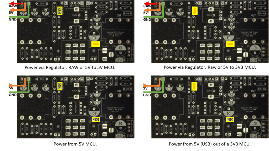
The “3V3 IO” jumper is there to control the audio levels sent to the microcontroller, not actually related to how either the PCB or microcontroller is powered itself.
The PCB circuit always requires 5V which can come from either the on-PCB regulator or a 5V output from a microcontroller. Any USB powered 3V3 microcontroller usually provides access to the USB’s 5V supply.
The power provided to the microcontroller can come from either the 5V line (from the regulator) or the RAW power input from the barrel jack (typically 7-12V) – labelled VIN on the power jumper.
Some examples:
- Arduino Nano: Use the VIN (RAW) output connected to the Nano’s VIN.
- Raspberry Pi Pico: Use the 5V output connected to the Pico’s VSYS.
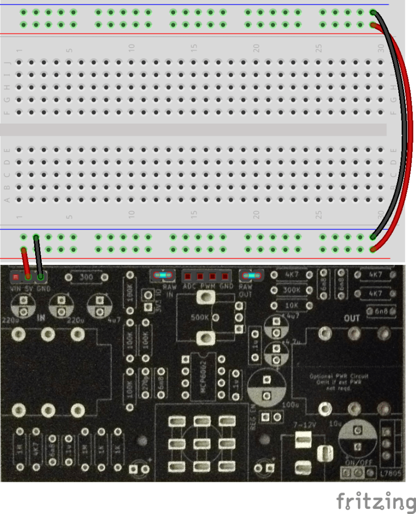
Powering the Breadboard from the Regulator
The power rails of the solderless breadboard can be powered from the PCB using the 5V and GND from the PCB-based regulator.
This is useful for prototyping circuits that do not require a microcontroller.
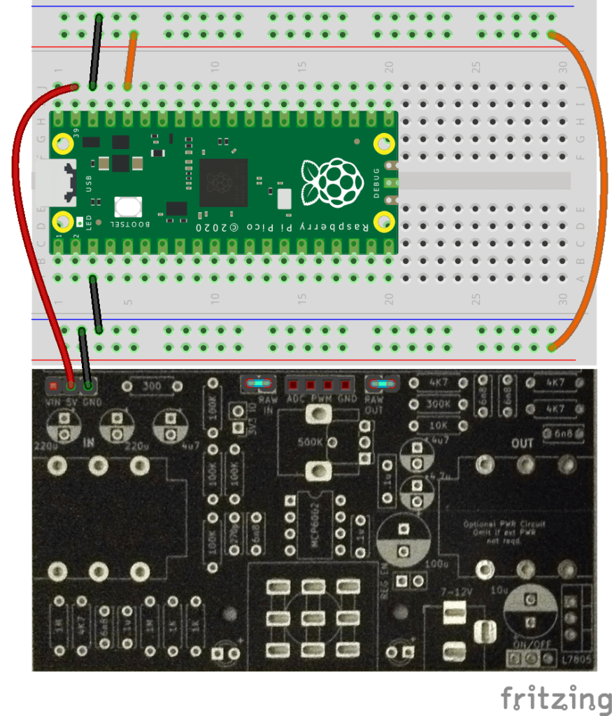
Powering the Breadboard from the Regulator with an MCU
If a 3V3 microcontroller is being used, then the breadboard should be powered from the microcontrollers 3V3 output instead. Otherwise, the 5V line from the regulator can be used as before.
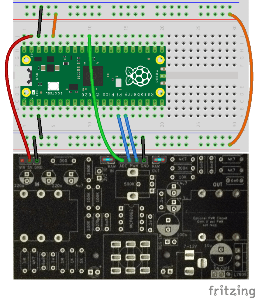
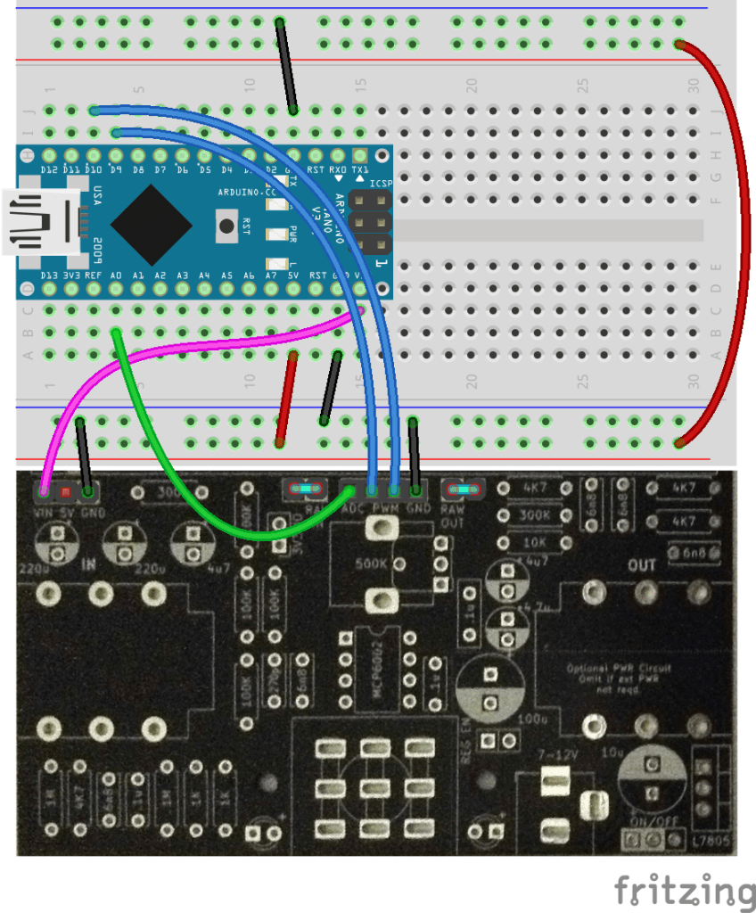
Here is how to use a Raspberry Pi Pico (5V to VSYS, then 3V3 to breadboard) and an Arduino Nano (VIN to VIN then 5V to breadboard).
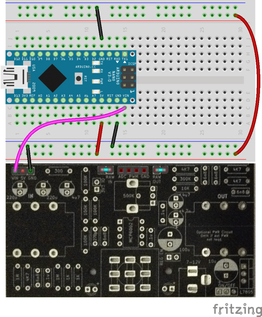
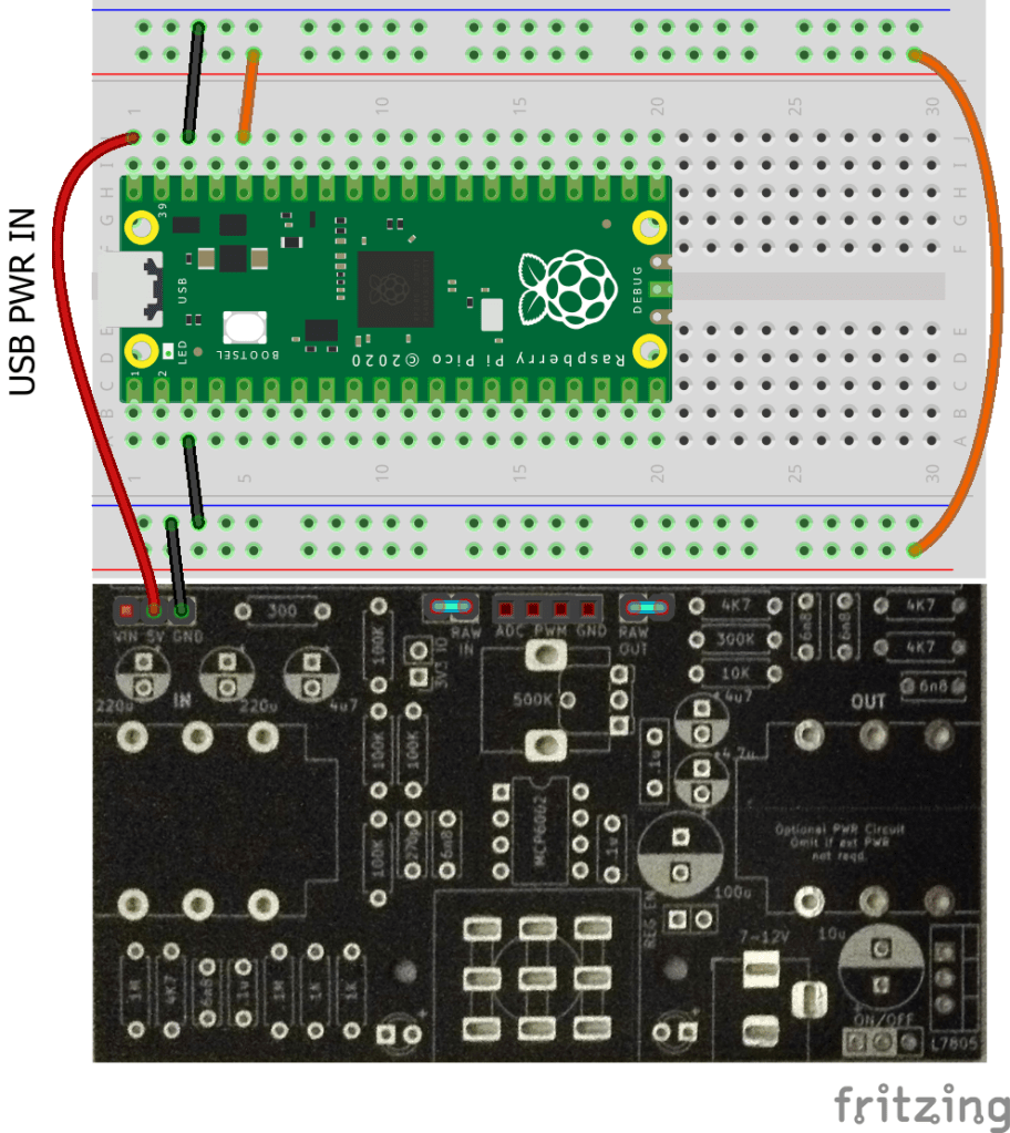
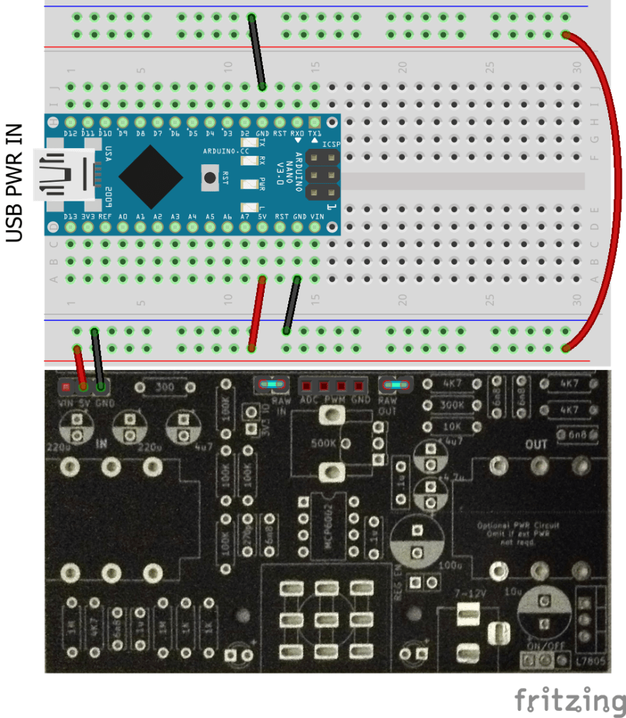
Powering the Breadboard from the MCU’s USB
It is possible to power the PCB and breadboard from the microcontroller’s 5V USB connection.
IMPORTANT: As previously mentioned, ensure the “REG EN” jumper is removed to prevent any possible “back powering” of the regulator.
The following shows how to do this with a Raspberry Pi Pico (VBUS to 5V, 3V3 to breadboard) and an Arduino Nano (5V to 5V, 5V to breadboard).
Powering the Prototyping Area
If the prototyping area is being used then there are two solder bridges that can be used to connect one or both positive power rails to 5V and one or both negative rails to GND.
By default the prototyping rails are NOT connected to anything else.
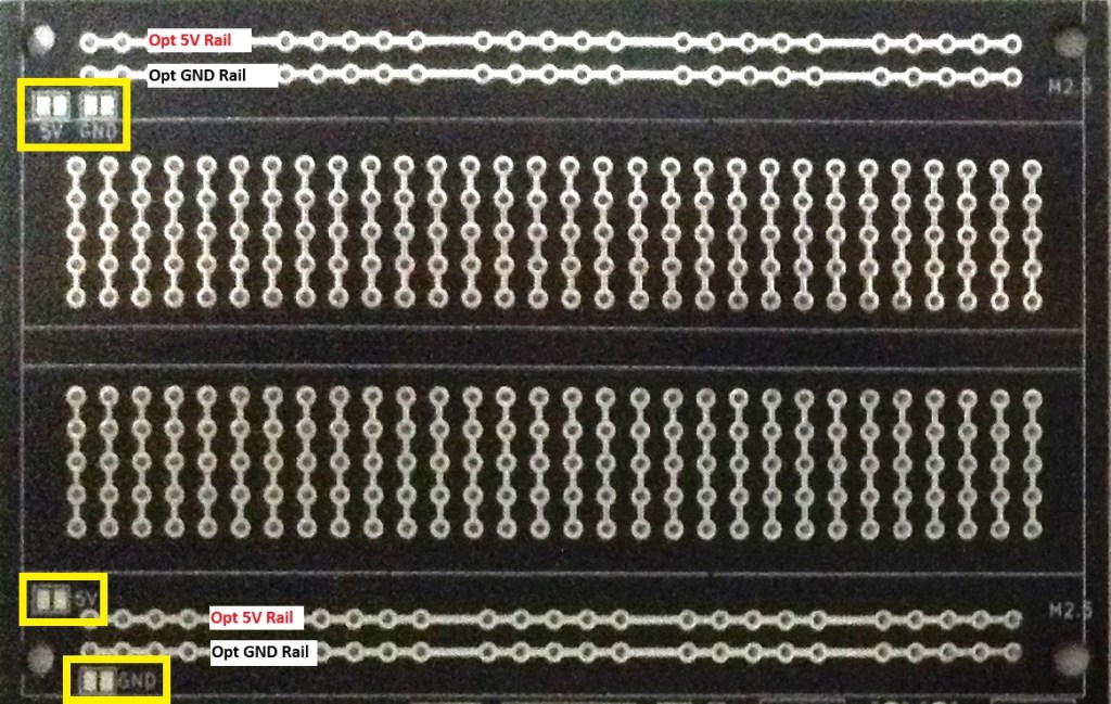
Patching into 5V or GND is left as an option to allow for the use of a 5V, 3V3 or no microcontroller as required.
The prototyping area is principally there to allow for easy mapping of a solderless breadboard design over to a soldered design. In that respect, the connections between the prototyping area and the VIN-5V-GND jumper would be the same as when using the breadboard.
The solder bridges are provided as a convenience for when a simple 5V power scheme is in use to avoid the need for longer wires to the power rails.
Audio Connection Options
There is a 4-way header socket to provide links between the PCB-based circuitry and the breadboard. There are two additional jumpers that enable access to the “raw” audio signal too, bypassing the PCB-based circuitry, but still subject to the “stomp” switch bypass action.
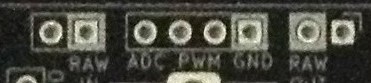
The headers are (from left to right):
- RAW INPUT jumper (jumper on = link to ADC input circuit).
- Connection to MCU ADC.
- Connection from MCU PWM: PWM0 then PWM1.
- GND
- RAW OUTPUT jumper (jumper on = link to PWM output filter circuit).
Audio Input
The PCB includes a pre-amp stage to take a guitar signal level and amplify it up to something that is useful for a microcontroller’s analog input. The potentiometer is used to set the gain and some experimentation is likely to be required.
The ADC signal will be DC biased to 2.5V (3V3_IO jumper off) or ~1.7V (3V3_IO jumper on) with the peak to peak amplitude set by the gain potentiometer. If the gain is set too high then clipping will occur at 0V and 5V in either mode.
If a microcontroller isn’t being used and access to the RAW guitar signal is required, then it can be obtained by removing the RAW IN jumper and patching a jumper wire to the RAW pin.
Note that the “stomp” bypass switch will still operate on the RAW signal too.
Audio Output
For output, it is possible to provide a dual PWM signal output which then passes through a filter and buffer before hitting the output jack.
Again, if a microcontroller isn’t being used then a RAW signal can be sent out by removing the RAW OUT jumper and patching a jumper wire directly to the RAW OUT pin. And again the “stomp” bypass switch will still act on the RAW signal.
The PWM output assumes the use of two GPIO pins to provide additional resolution to the digital to analog conversion. The theory is fully described in this tutorial from Open Music Labs.
The short version is that the two outputs are effectively a “most significant byte” and “least significant byte” which are then summed. Key to this working is the ratio of the two resistors used in the mixing, which is why 1% tolerance resistors were used to try to keep this ratio as accurate as (economically) possible.
Referring back to the schematic and comparing it with the notes from Open Music Labs:
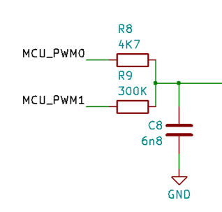
We can see that the ratio of resistors is given by 4,700 / 300,000 which is pretty close to 64. This is 2^6 so it is allowing for a 12-bit audio output resolution with the most significant 6-bits on PWM0 and the least significant 6-bits on PWM1.
When used with the 6.8nF capacitor, we end up with a cut-off frequency (again see the OML tutorial) for the filter of:
freq = 1 / (2.PI.R.C) = 1 / (2 x PI x 4,700 x 0.000,000,006,8) ~= 5KHz
This is essentially what Electro-smash did for their PedalPi. Their original PedalShield used a larger resistor for PWM1 (1M2) and aimed for twin 8-bit resolution.
Example Microcontroller Audio Connections
Here are examples using the Raspberry Pi Pico (ADC0, GPIO10, GPIO9) and an Arduino Nano (A0, D9, D10).
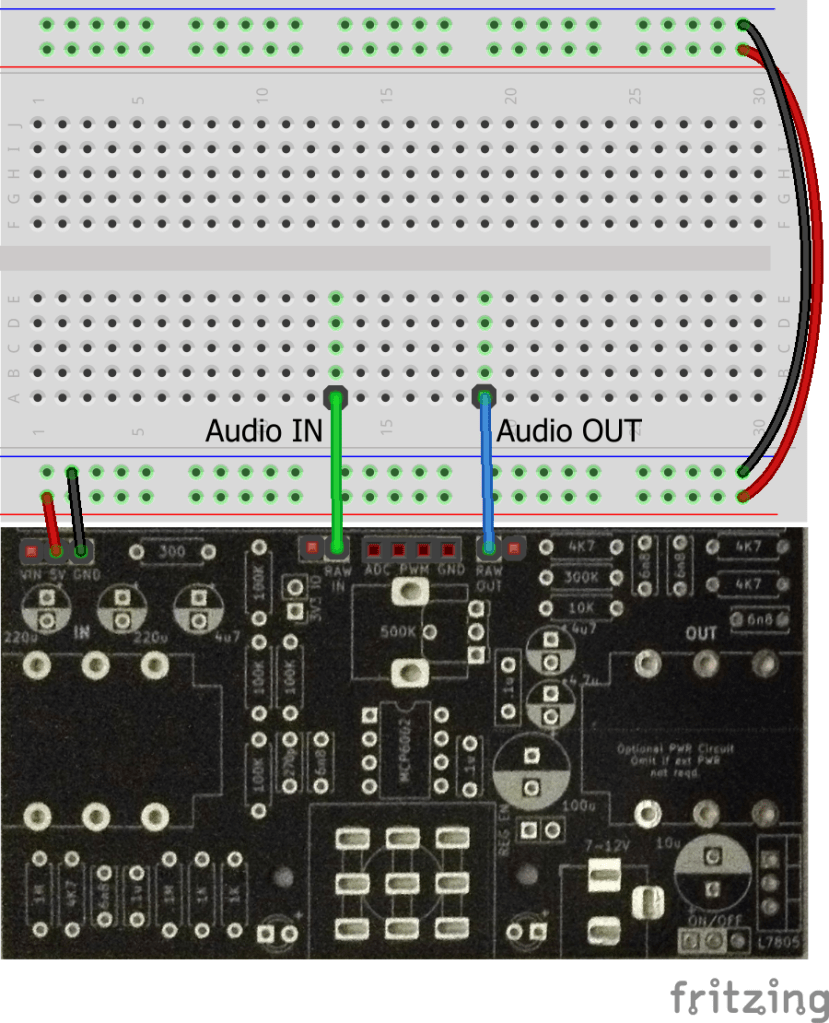
RAW Audio Input and Output
Removing the RAW jumpers gives access to the unprocessed, raw audio from the IN jack and direct access back to the OUT jack. As previously mentioned the “stomp” bypass switch will still function on the RAW signals – i.e. it will enable or disable the RAW signals as part of the bypass function.
If the pre-amp is required, then the ADC pin can be used for the amplified input and then the output still sent directly to the OUT jack if required.
Example Arduino Software Pass-through
Using the Arduino Nano audio link up as shown above a simple audio-passthrough test can be performed by configuring PWM access on pins D9 and D10, which both use Timer 1, and then taking the value read from an analog input and writing out over PWM.
To configure PWM for both pins requires the following code:
void initPwm() {
  pinMode(9, OUTPUT);  // OC1A output
  pinMode(10, OUTPUT); // OC1B output
  TCCR1A = _BV(COM1A1) | _BV(COM1B1) | _BV(WGM11);
  TCCR1B = _BV(WGM13) | _BV(WGM12) | _BV(CS10);
  TCCR1C = 0;
  ICR1 = 63; // 6-bit resolution
}
This configures Timer 1 for Fast PWM Mode, running at the MCU system clock speed (no “prescalar”) with outputs enabled for OC1A (D9) and OC1B (D10). The resolution for PWM is set to 6-bits, so the internal counter will count from 0 to 63 and then reset.
This means that software can write a value between 0 and 63 to the OCR1A or OCR1B registers to set the duty cycle for the PWM output between 0 and full. To write out a full 12-bit value requires splitting over these two registers as follows:
void setPwm (uint16_t pwmval) {
  OCR1A = pwmval >> 6;   // Most significant 6-bits
  OCR1B = pwmval & 0x3F; // Least significant 6-bits
}
Then it is simply a case of free-running in a loop a continual read of the analog input and write out to PWM, converting the 10-bit analog value to a 12-bit value on the way.
void setup() {
  initPwm();
}

void loop() {
  uint16_t val = analogRead(A0);
  setPwm (val<<2);
}
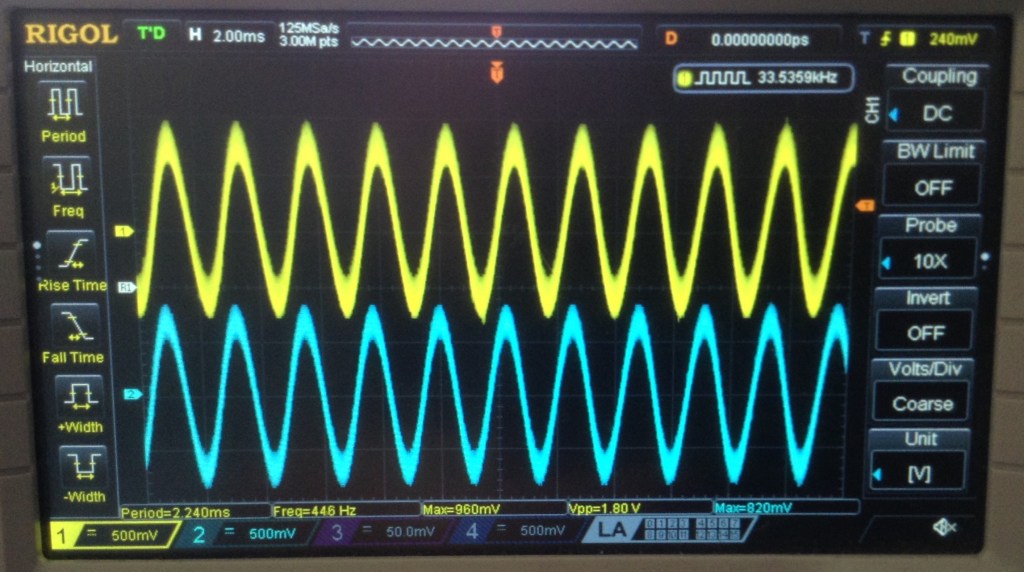
In the following trace the blue trace is the signal at the IN jack and the yellow trace is the signal at the OUT jack. The gain has been adjusted to make them essentially the same amplitude.
Closing Thoughts
This is a new venture for me, so it remains to be seen if this is actually any good!
But a massive thanks must go to Electro-smash for their PedalShield and PedalPi projects, and for open sourcing the designs, as that information has given quite a leap forward in even starting on my own design – most of the analog circuitry is based on PedalPi.
I might have been tempted to have just bought one of their kits, but they are not currently available (in the UK at least).
But this way, it gives me a chance to learn some new things and make some (more) new mistakes.
Kevin
