Here are the build notes for my Proto Pedal PCB Design.
- Part 1 – PCB Design and Introduction.
- Part 2 – PCB Build Guide.
- Part 3 – Proto Pedal Usage and Application Notes.

Warning! I strongly recommend using old or second hand equipment for your experiments. I am not responsible for any damage to expensive instruments!
If you are new to electronics, see the Getting Started pages.
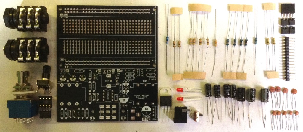
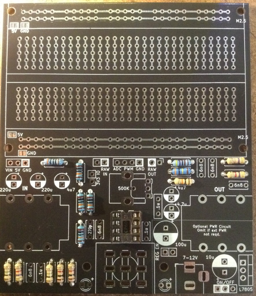
Bill of Materials
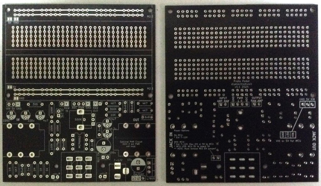
- Proto Pedal PCB (GitHub link below)
- 1x MCP6002 dual opamp.
- General Resistors: 1x 300Ω, 2x 1K, 3x 4K7, 1x 10K, 4x 100K, 2x 1MΩ.
- 1% Tolerance Resistors: 3x 4K7, 1x 300K.
- 1x 500KΩ pcb mount potentiometer.
- Ceramic capacitors: 1x 270pF, 5x 6n8, 3x 100nF.
- Electrolytic capacitors: 3x 4u7, 2x 200uF.
- 2x LEDs.
- 1x 4-way pin header socket.
- Pin headers
- 3x jumpers.
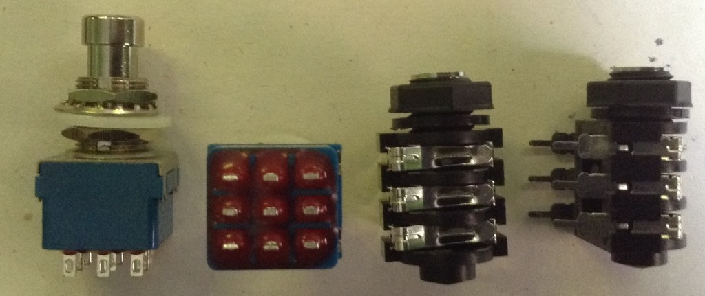
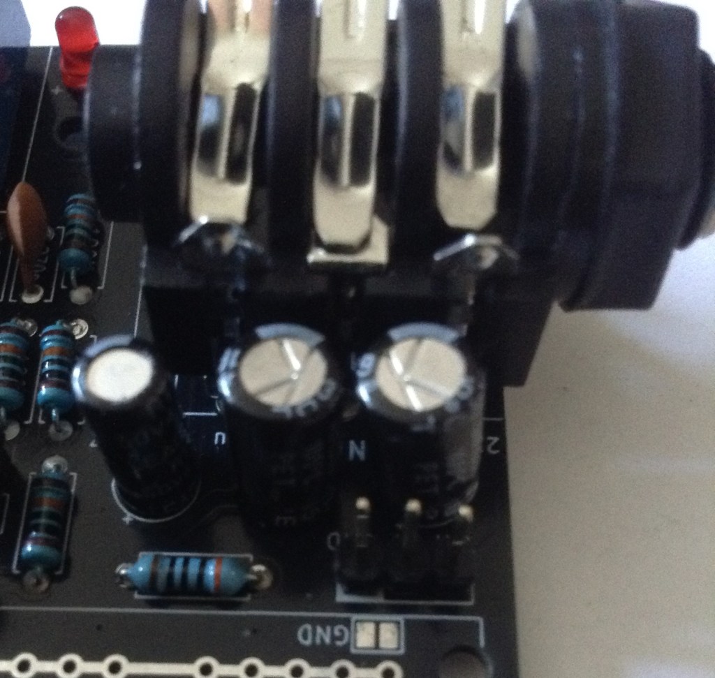
- 2x PCB mount std jack (1/4″) stereo or mono jack sockets (see photo).
- 1x 3PDT “stomp” switch (see photo).
- Optional: 1x 8-way DIP socket.
Additional components for the 5V power supply circuit:
- 1x LM7805 regulator
- Electrolytic capacitors: 1x 10uF, 1x 100uF.
- 1x slider switch (2.54mm pitch).
- 1x 2.1mm barrel jack socket.
- 1x 2-pin header and jumper.
If the board is to be powered from a microcontroller on the breadboard area then the power supply circuit can be omitted.
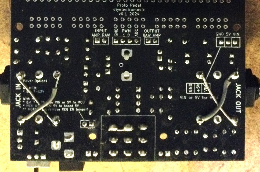
Note: The footprints for the jack sockets are the wrong way round, but I’ll show how some patch wires need to be applied shortly.
Build Steps
Taking a typical “low to high” soldering approach, this is the suggested order of assembly:
- All resistors.
- DIP socket (if used).
- Disc capacitors.
- LEDs.
- 4-way header socket.
- Pin headers
- Electrolytic capacitor.
- Jack sockets.
- Potentiometers.
- Stomp switch (see the note about the wiring below).
- Patch wires for the jacks.
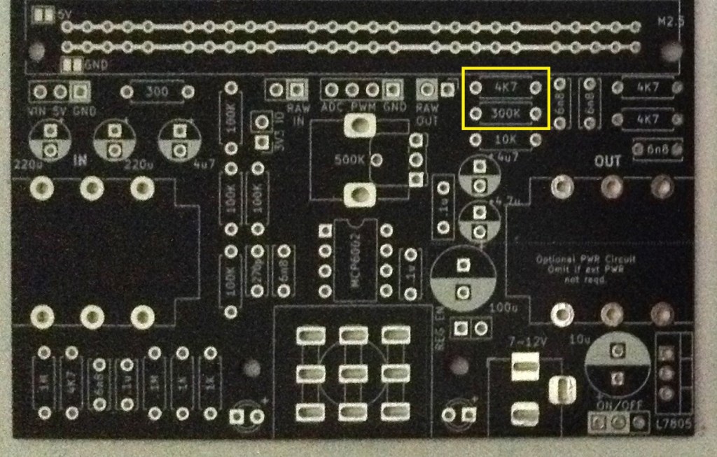
As there are a number of different values for resistors and capacitors extra care is required to ensure the right values go in the right places.
The two 1% resistors are highlighted below. These are required for better accuracy for the PWM output option.
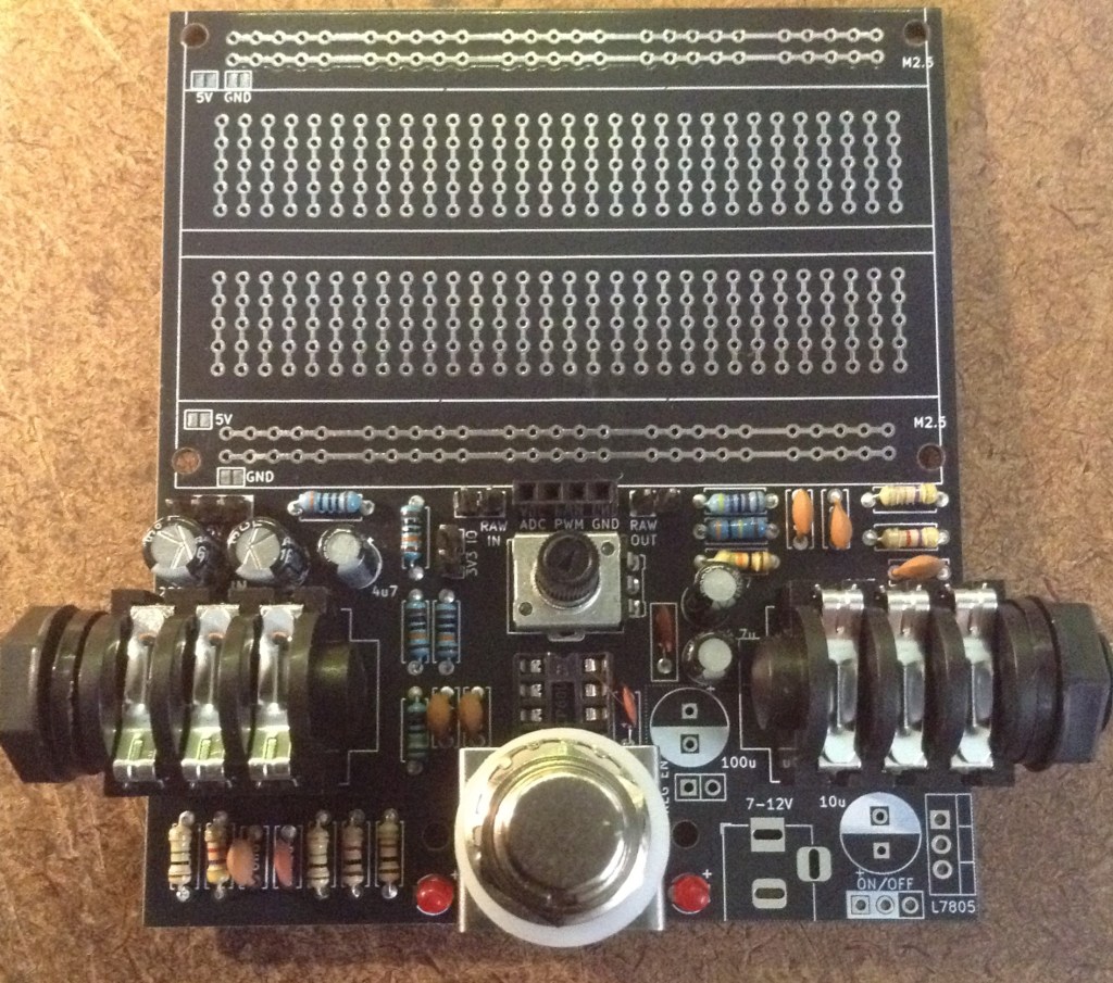
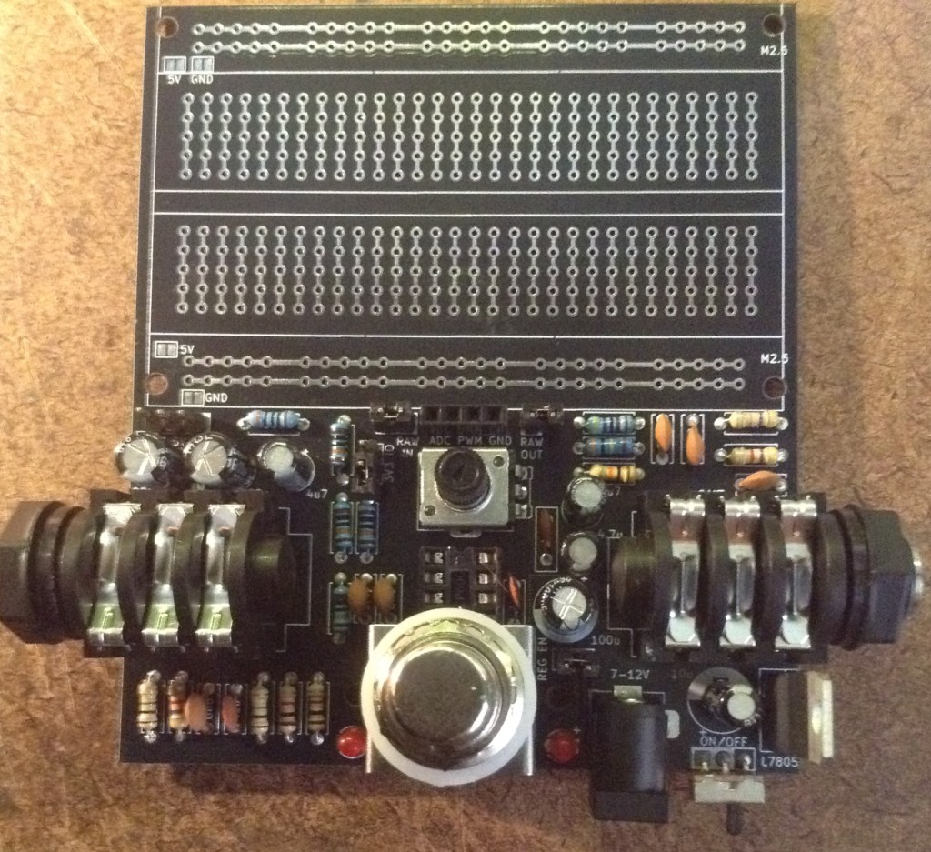
Here are some build photos.
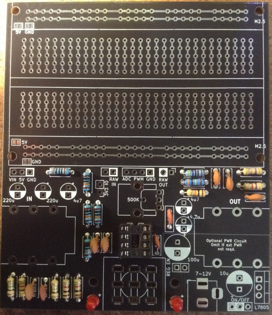
Note in my first build I soldered on the electrolytic capacitors before the headers. It is actually a lot easier to do this the other way round! I recommend soldering the pin headers first.
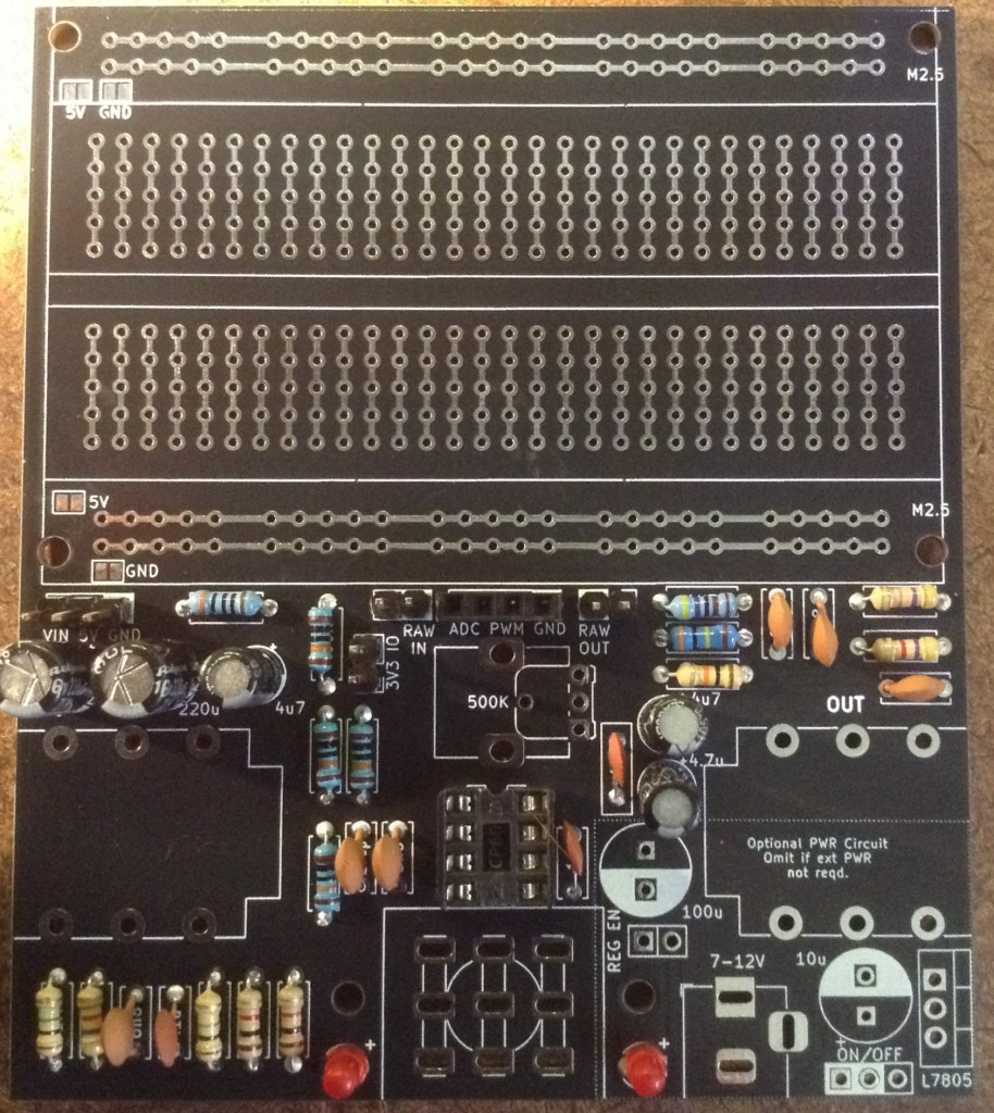
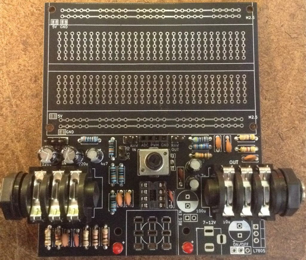
If you know you’re adding the power supply then it is worth adding those components as you go. This first build shows a board with no power supply (left) and one with (right).
Important: if the patch to adjust the wiring of the 3PDT switch is being used, then the track on the top of the board has to be cut prior to soldering on the switch!
Once everything else is complete, some patch wires are required on the jack sockets to correctly hook them up to the pedal as shown below.
At this stage, then if there is no jack plugged into the OUT socket, activating the bypass will GND the signal at the IN jack via the switched connectors in the jack sockets.
This means that anything plugged into the IN jack at this point will essentially see zero impedance. That might be ok with a passive pickup, but I’m sure that would be problematic with any kind of active set-up – shorting the output straight to GND doesn’t sound like a good thing to me.
One option is to always ensure there is something plugged in to the OUT jack – e.g. a std jack adaptor or something.
But it is possible to solve this by bending away the switched contacts on the jack sockets as shown below. This is a little tricky and involves bending away the larger contacts and then bending them back, but it can be done.
3PDT Alternative Wiring
As mentioned in the design notes, I was actually planning on using a slightly different wiring for the 3PDT “stomp” switch in order to implement the “true bypass” option.
This can still be achieved on this board by applying the following patch prior to adding components.
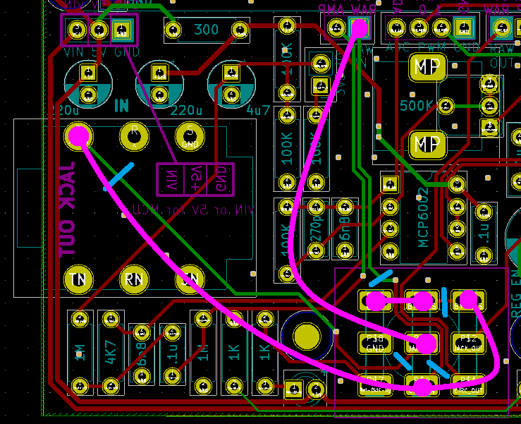
The blue lines show where a trace has to be cut. There are two on the underside of the board (which an alternative option on top) and one (only) on the top. Any top traces have to be cut prior to soldering down the stomp switch.
The four magenta lines show additional wiring that is required to reimplement the true bypass once the tracks have been cut.
I’ve not tested this patch yet. For now, I’m just going with the PCB “as is”.
Testing
I recommend performing the general tests described here: PCBs.
To test the input stage requires a signal and ideally an oscilloscope. The input signal vs the signal at the “ADC” pin header can be checked to verify the following:
- That a signal isn’t passed through when the bypass switch is activated (LED off).
- That a signal is passed through when the bypass switch is not activated (LED on).
- That the potentiometer can be seen to adjust the gain up to a maximum of almost 5V peak to peak.
- When the 3V3_IO jumper is off, the ADC signal is DC biased by 2.5V.
- When the 3V3_IO jumper is on, the ADC signal is DC biased by around 1.7V.
To test the PWM output, use the Arduino Software Pass-through Test described in the Proto Pedal PCB Usage Notes.
PCB Errata
In summary, there are the following issues with this PCB:
- The breadboard footprint should have solder mask over the adjoining pads between the holes.
- The two standard jack sockets are mounted back to front.
- The wiring for the 3PDT switch is sub-optimal, but probably ok (see design notes).
Enhancements:
- It would have been useful to highlight the 1% resistors on the silkscreen.
- The LEDs are a little bright…
Find it on GitHub here – tbd.
Find the application and usage notes here.
Closing Thoughts
Despite the issues, I’m actually really pleased with how this has come out. I’ve only just started to put together the various options for how this can be used, so I expect there will be additional errata come out as I realise the other mistakes I’ve made, but so far (switch issue not withstanding) this seems to be manageable.
It is annoying that the jack footprint wasn’t obvious which way round it should go, although I can see how the silkscreen does sort of relate to the layout of the socket. What is annoying is that I hadn’t spotted that the signal track was going to (obviously with hindsight) the connector of the socket that makes contact with the shield.
I think this will be a useful platform as it stands for further experimentation now for me, but I can’t imagine anyone else being interested with it until the issues have been fixed.
Kevin
