I’ve now done several posts inspired by the Oskitone Poly 555, and I do plan to build one myself one day (I can’t get a kit as they don’t deliver to the UK, but I’ve had a PCB manufactured – watch this space!).
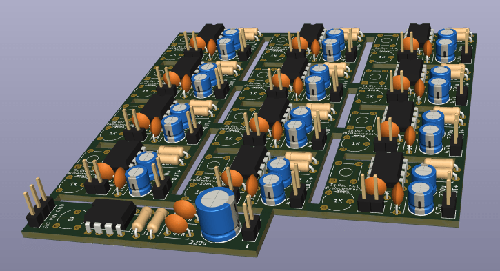
This PCB is essentially the oscillator part of the Poly 555 in an independent unit. I wanted several “single button” oscillators that I could do something different with at some point, but as they turned out so small, I paneled them up and this was the result.
I’m not sure I’d recommend anyone else attempting to use this PCB, but as always all my design thoughts and results will be published regardless.
- The Build Guide is available here: Simple Square Wave Oscillator PCB Build Guide
Warning! I strongly recommend using old or second hand equipment for your experiments. I am not responsible for any damage to expensive instruments!
These are the key Arduino tutorials for the main concepts used in this project:
If you are new to electronics, see the Getting Started pages.
The Circuit
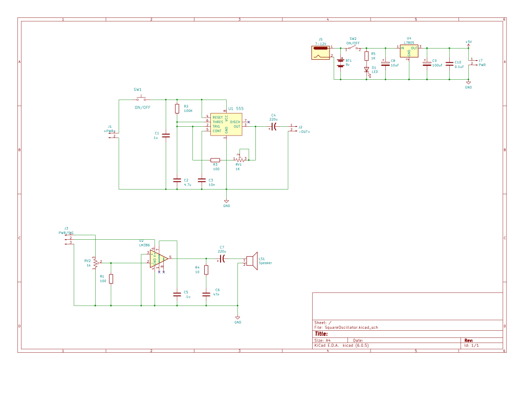
This essentially the schematic for a single oscillator from the Poly 555 but with a few minor tweaks:
- The oscillator is tuned with a trim pot and triggered with a tactile button switch (like the original).
- I’ve removed the LED and associated resistor.
- I’ve added a coupling capacitor on the output rather than a mixing resistor.
- There are two sets of pin headers, one for power and one for the speaker.
- I’ve built up the mixing amp section as an independent board in case I want to link several oscillators together.
My thinking is that if I did want to tie the audio outputs together I can replace the coupling capacitor with a 10K resistor and feed the outputs into the amp section, mirroring what would happen in the original unit.
The original included a power section to drop the 9V battery supply down to 5V for use with the oscillators. I’ve included that in the schematic but ended up not actually using it myself on the PCB.
Once again, from a 9V supply, I am assuming the use of a recycled headphone speaker with an impedance of around 40Ω, giving me a maximum current of 9V/40Ω = 225mA, which might be just about ok…
But as the 555 typically has a maximum current sink/source of 200mA, there really ought to be an additional resistor in series with the speaker. A total resistance of just 45Ω would limit the current to 200mA at 9V.
Alternatively, using a 6V supply (e.g. 4 AA batteries) would mean 6V/40Ω = 150mA so that would be fine too as I understand things.
Either way, once again this is a board for experimentation, assuming some knowledge (ideally more than mine) of electronics and must NOT be plugged into anything of value and especially anything expecting audio or headphone level signals.
PCB Design
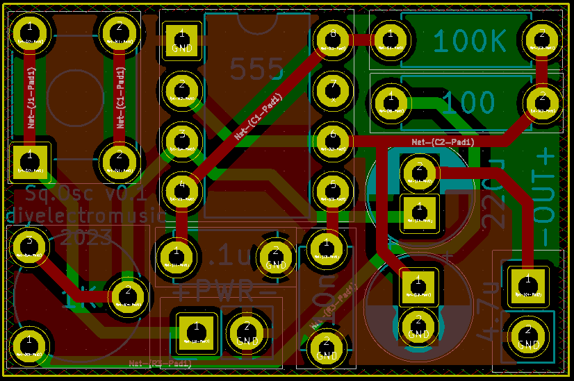
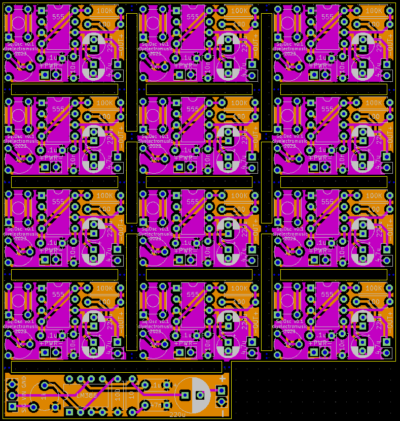
This is a relatively straight forward design. I’ve opted for the smallest footprint I thought I could get away with and then tiled them up to give me 12 boards (i.e. enough for an octave if I wanted) in a 100x100mm footprint.
I did manage to get a footprint mismatch between the schematic and the PCB though, resulting in the switch not actually getting connected to the 555! This means a single, small patch link is required, but more on that in the build guide.
I also decided to include the optional amp section, but because I’d added “stamp holes” between the boards, this was picked up at the design review and flagged as a second design on the PCB. At this point I had three options:
- Re-submit the gerber files containing just a single design.
- Agree to make all the internal cuts myself.
- Pay extra to include the additional design as submitted.
In previous designs, I’ve had optional parts of the board, but as they were always linked with rigid (i.e. no perforations or “stamp holes”) parts of PCB, and often with a common GND zone too, they’ve not been flagged before.
In the end I just paid the extra and chalked this one up to a learning experience. There were too many internal cuts to consider making those myself, and I didn’t really want to rework the board.
So for Seeed Fusion, it seems I can panel and use stamp holes as long as it is obviously a single design; or I can have a range of optional elements for a board, as long as there aren’t stamp holes, V-cuts, milled holes, or other obvious “special workings” to make them “snappable”, and they are genuinely optional elements with common GND, power, and so on.
Closing Thoughts
As I’ve said many times, I am not really an electronics person, so everything I do and document on this blog is part of me experimenting and learning. And the best way to do that is learning from others successful designs, so a massive thanks to Tommy from Oskitone for publishing the design of the Poly 555 as an opensource hardware project.
But along the way I will make mistakes, misunderstand something, or just simply not quite realise how something works. In this case I’ve learned a little more about what is appropriate in terms of sending PCBs for manufacture, and whilst I ended with an extra charge (which I just met directly in this case) it was interesting to see how the design review stage works.
These boards have been sent to be manufactured by the Seeed Fusion PCB service, which I am happy to continue to recommend. They have been supported with discount vouchers that I’ve been sent by Seeed for my previous projects.
Kevin
