This is the build guide for my Raspberry Pi v1 Model B Synth Board PCB.
Warning! I strongly recommend using old or second hand equipment for your experiments. I am not responsible for any damage to expensive instruments!
If you are new to microcontrollers, single board computers and electronics, then see the Getting Started pages.
Bill of Materials
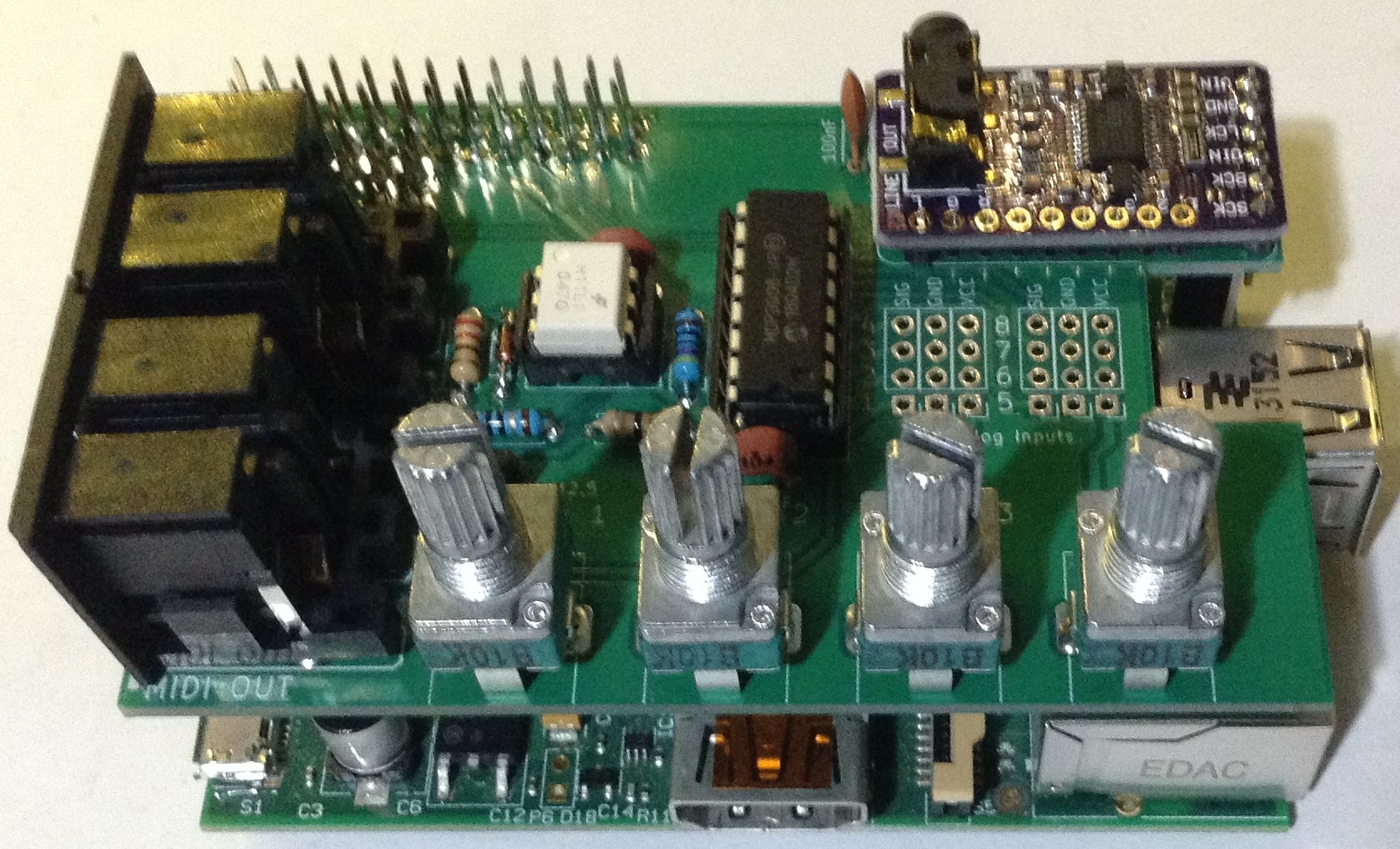
- Raspberry Pi v1 Model B Synth Board PCB (GitHub link below).
- GY-PCM5102 DAC module.
- H11L1 optoisolator.
- MCP8003 SPI ADC.
- 1x 220Ω resistor.
- 1x 470Ω resistor.
- 1x 33Ω resistor.
- 1x 10Ω resistor.
- 1x 1N914 or 1N4148 signal diode.
- 3x 100nF ceramic capacitors.
- Optional: 4x 10KΩ linear (“type B”) potentiometers – PCB mount (see photos for footprint).
- 2x 5-pin 180 degree DIN sockets – PCB mount (see photos for footprint).
- Optional: 1×6-way DIP socket.
- Optional: 1×16-way DIP socket.
- 1x 26-way extended GPIO header.
- 2x 4-way extended pin header sockets.
- Pin headers.
- 2x 2.5mm, 18mm stand-offs (M-F), nuts and screws.
And of course, a Raspberry Pi V1 Model B (26-way GPIO version, with the additional 8-way P5 header) and SD card, power, etc, to use it with.

Build Steps
The build should proceed in a “low to high” manner. This is the suggested soldering sequence:
- The resistors and diode.
- The two DIP sockets if used.
- The capacitors.
- The GY-PCM5102 module.
- The GPIO and P5 header sockets.
- The MIDI DIN sockets.
- The potentiometers (if used).
Finally the H11L1 and MCP3008 can be added. Note that the orientation of the two devices is in opposite directions – one up and one down.
In the photos below I soldered the MIDI sockets and potentiometers before the GPIO header sockets and then wished I’d done it the other way round!
Warning: Before affixing the GY-PCM5102 module, ensure the solder bridges are configured correctly on the underside of the board (details of the required configuration can be found here) and ideally test the module prior to soldering down.


Getting the alignment of the GPIO and P5 headers correct was a little tricky. Ideally the additional pin headers for the P5 header would be added to the Raspberry Pi first and then that used as a guide for the sockets on the IO board.
It may be necessary to add additional spacers to the GPIO headers to ensure there is enough clearance above the ethernet socket. In my case I needed one additional layer that I grabbed from some old pin headers as shown below. This fitted the use of 18mm stand-offs quite nicely too.

Once the P5 header pins have been added to the Pi, they should align with the other pins on the GPIO connector as shown below.

This can then be used to align the pin header sockets for the GPIO and P5 connectors on the IO board too.


Note that when mounting the board, it is recommended that two 18mm, 2.5mm stand-offs are used. One of these will sit underneath the PCM5102 module though, where there is no hole, so it will have to just rest and support, but not be connected. The other one can be fully screwed in top and bottom to secure the IO board to the Pi.

Board Options
The photos above show the board being used with four potentiometers. This requires the use of extended headers to ensure that the underside of the IO board (and pots) doesn’t touch the Pi’s ethernet socket. If required, the last pot (#4) could be left off.
Alternatively, there are 8 sets of pin headers that provide a SIG-GND-VCC connection for each of eight external potentiometers.

GPIO Usage and Software Interface
The MCP8003 is connected to SPI bus 0 and uses CE1 as the chip select. MIDI is on RXD/TXD and the PCM5102 DAC is connected to I2S via the P5 header.
The following GPIO are used in total:
- GPIO7 (CE1) to MPC3008 CS
- GPIO9 (CISO) to MCP3008 DOUT (used to be called MISO)
- GPIO10 (COSI) to MCP3008 DIN (used to be called MOSI)
- GPIO11 (SCLK) to MCP3008 CLK
- GPIO14 (TXD) to MIDI OUT
- GPIO15 (RXD) to MIDI IN
- P5-GPIO28 (I2S/BCLK) to PCM5102 BCK
- P5-GPIO29 (I2S/LRCLK) to PCM5102 LCK
- P5-GPIO31 (I2S/DATA) to PCM5102 DIN

Testing
I recommend performing the general tests described here: PCBs.
PCB Errata
There are no errata to be aware of as far as I know at present.
If I was to redesign the board, then I might consider the following changes:
- Update the footprint of the MIDI sockets to use rectangular pads for additional strength.
- Even though the second mounting hole is beneath the PCM5102, I would probably still add it to the IO board anyway.
- There might even be space for a proper buffered 74HCT14 MIDI output stage which would be much better.
Closing Thoughts
I’m pretty pleased with this board now. All functions seem to work. The test code I have is still pretty primitive, so I need to get back to work on that, but as a platform for some future experimentation this is a lot neater than my original proto-board prototype!
These boards have been manufactured using the Seeed Fusion PCB service, which I am happy to continue to recommend. They have been supported with discount vouchers that I’ve been sent by Seeed for my previous projects.
Kevin